RLV12 V2.0 Background
As mentioned the RLV12 Emulator V1.0 did come with some flaws that make it less easy to use. Most notably the programming interfaces for the AVR MCU (ISP) and the CPLD (JTAG) are virtually inaccessible when the card is plugged into a Q-Bus backplane. Also the SD-Card could not really be accessed from outside without using tweezers. And last but not least the console for the emulator required a special cable.
The bus Q-Bus receivers DS8837 I used, especially in a SOIC SMD package, are virtually unavailable. They have been replaced with the solution implemented on my memory board uinsg 47HC4049 operated at approximatively 3.3V.
The bidirectional Q-Bus transceivers, digital DC005N aka Signetics C2324N, as well are very difficult to find and as well often very expensive. They have been replaced with 74HC4049 for the receiving direction and with 74F38 for the transmitting direction.
To make it easier to build your own emulator I switched the design to an (almost) all through hole design, avoiding SMD parts as much as possible. Most notably the TQFP-100 package with only a 0.5mm pitch, which is difficult to solder without the proper equipment and sufficient experience.
This required me to use PLCC packages for the CPLD and PLCC sockets. However the ATF1508 in a PLCC‑84 package has less usable pins and at the same time the new design for the transceivers required more pins as they require a separate 16‑bit bus to transmit or receive the bus signals BDAL0..15.
Therefore I had to add a second CPLD, a ATF1504 in a PLCC‑44 package. As a result I now had more resources available and so could implement a DMA data register to speed up DMA
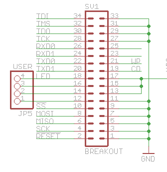
To solve the issue with the accessibility of the programming interfaces, the serial command line interface and the SD-Card I have added a break-out board that connects to the RLV12 Emulator via an 34‑pin IDC cable.
The Break-Out Board
Here is a picture of the first break-out board version. This will in fact be the general standard break-out board for all of my ongoing designs, not only for the Q-Bus cards but as well for my PDP-11/Hack. Note the break-out is still all SMD because the SD-Card cages are only available as SMD parts, so it does not make sense to avoid other SMD parts with more or less the same difficulty to solder as the SD-Card cage. In addition SMD parts save a lot of sapce.
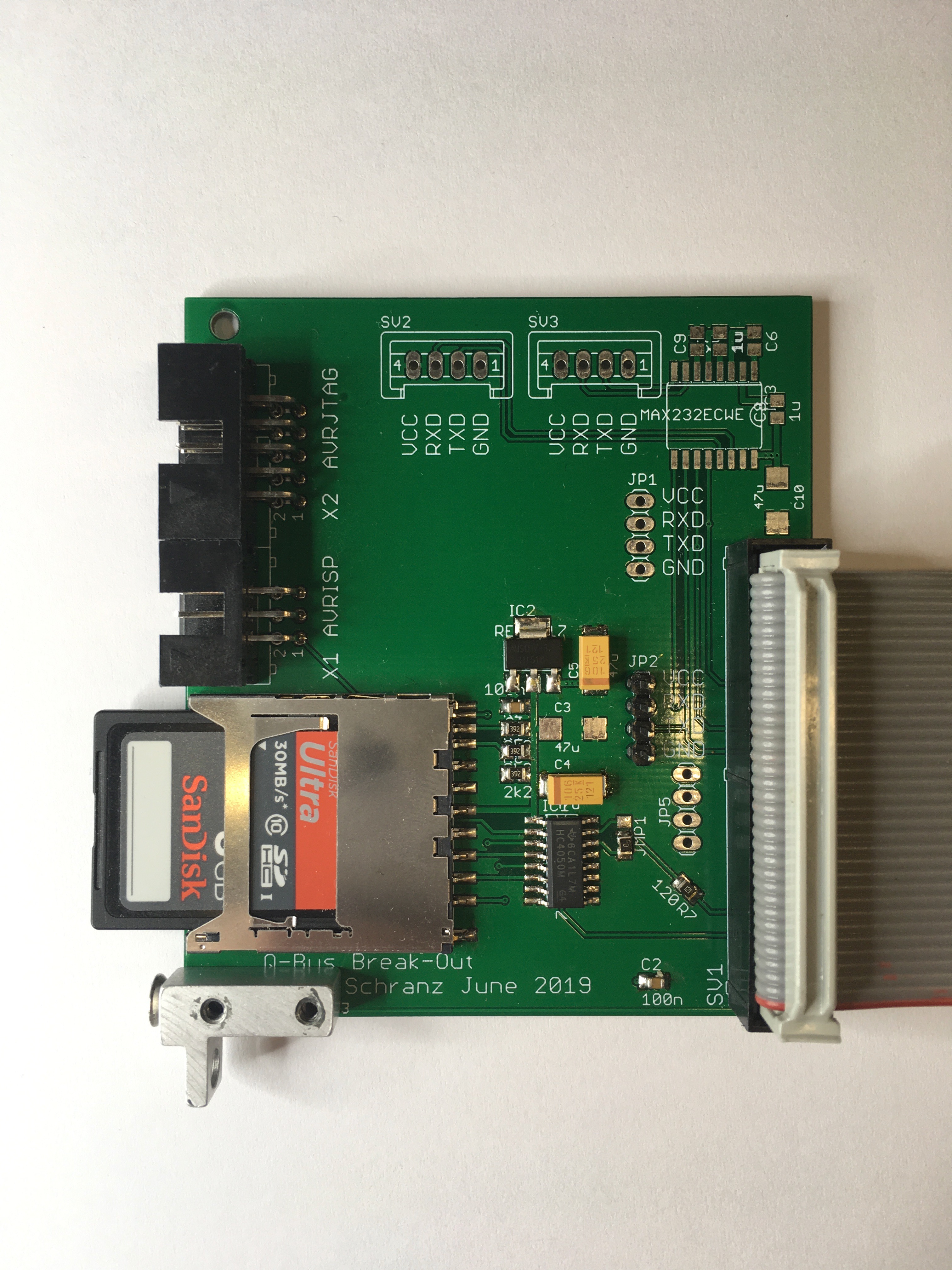
The layout of the 34-pin IDC is fixed and has dedicated signals for the ISP, JTAG and up to 4 serial interfaces. It also includes signals for CD (Card Detect) and WP (Write Protect) and 4 user defined signals. I intend to make this the standard break-out board for most of my designs.