RLV12 V2.0 Building Instructions
Introduction
The RLV12 Emulator Version 2.0 consists of a short dual-width Q-Bus card and a breakout board. The two prints are connected via a 34-pin ribbon cable. The break-out board has the SD-Card cage, the AVR ISP Header and the Atmel CPLD JTAG interface. It also brings the serial port from the MCU either directly as TTL signals to a 4-pin header or via a MAX232 levelshifter to a connector.
The layout has been designed to fit on a filler panel of a BA23 case. When using the MAX232 you must add a DB-9 connector to the filler panel and wire the pins 2,3 and 5 with the connector that carries the signal from/to the MAX232 RS-232 level shifter. Please make sure to place RX and TX according the type of connector, male or female, you are using.
BOM Bill of Materials
| Name | Value | Package | Description |
| C1 | 330n | C0805 | Decoupling Capacitor |
| C2 | 330n | C0805 | Decoupling Capacitor |
| C3 | 330n | C0805 | Decoupling Capacitor |
| C4 | 1u | C0805 | Decoupling Capacitor |
| C5 | 220n | C0805 | Decoupling Capacitor |
| C6 | 220n | C0805 | Decoupling Capacitor |
| C7 | 220n | C0805 | Decoupling Capacitor |
| C8 | 220n | C0805 | Decoupling Capacitor |
| C9 | 22p | C0805 | X-TAL Load Capacitor |
| C10 | 22p | C0805 | X-TAL Load Capacitor |
| C11 | 220n | C0805 | Decoupling Capacitor |
| C12 | 220n | C0805 | Decoupling Capacitor |
| C13 | 220n | C0805 | Decoupling Capacitor |
| C14 | 220n | C0805 | Decoupling Capacitor |
| C15 | 220n | C0805 | Decoupling Capacitor |
| C16 | 220n | C0805 | Decoupling Capacitor |
| C17 | 220n | C0805 | Decoupling Capacitor |
| C18 | 220n | C0805 | Decoupling Capacitor |
| C19 | 330n | C0805 | Decoupling Capacitor |
| C20 | 330n | C0805 | Decoupling Capacitor |
| C21 | 47u | SMC_C | Decoupling Capacitor |
| C22 | 47u | SMC_C | Decoupling Capacitor |
| C23 | 47u | SMC_C | Decoupling Capacitor |
| C24 | 220n | C0805 | Decoupling Capacitor |
| C25 | 220n | C0805 | Decoupling Capacitor |
| C26 | 220n | C0805 | Decoupling Capacitor |
| C27 | 220n | C0805 | Decoupling Capacitor |
| C28 | 47u | E2,5-5 | Decoupling Capacitor |
| C29 | 47u | E2,5-5 | Decoupling Capacitor |
| C30 | 47u | E2,5-5 | Decoupling Capacitor |
| C31 | 47u | E2,5-5 | Decoupling Capacitor |
| C32 | 47u | E2,5-5 | Decoupling Capacitor |
| C33 | 47u | E2,5-5 | Decoupling Capacitor |
| C34 | 330n | C0805 | Decoupling Capacitor |
| C35 | 330n | C0805 | Decoupling Capacitor |
| C36 | 330n | C0805 | Decoupling Capacitor |
| E1 | 74S38N | DIL14 | Quad O.C. NAND Gate |
| E2 | 74S38N | DIL14 | Quad O.C. NAND Gate |
| E3 | 74S38N | DIL14 | Quad O.C. NAND Gate |
| E4 | 74S38N | DIL14 | Quad O.C. NAND Gate |
| IC1 | ATF1504AS-10JU44 | PLCC-44 | 64 Macrocell CPLD |
| IC2 | 74C4049N | DIL16 | Hex High-Voltage Input Buffer |
| IC3 | 74C4049N | DIL16 | Hex High-Voltage Input Buffer |
| IC4 | 74C4049N | DIL16 | Hex High-Voltage Input Buffer |
| IC6 | 74C4049N | DIL16 | Hex High-Voltage Input Buffer |
| IC7 | 74C4049N | DIL16 | Hex High-Voltage Input Buffer |
| IC8 | ATMEGA1284P-20PU | DIL40 | Microcontroller |
| IC9 | ATF1508AS-10JU84 | PLCC-84 | 128 Macrocell CPLD |
| IC10 | REG1117 | SOT223 | 3V3 LDO Voltage Regulator |
| IC11 | 74S38N | DIL14 | Quad O.C. NAND Gate |
| IC12 | 74S38N | DIL14 | Quad O.C. NAND Gate |
| IC13 | 74S38N | DIL14 | Quad O.C. NAND Gate |
| IC14 | 74S38N | DIL14 | Quad O.C. NAND Gate |
| Q1 | 22.1184MHz | HC49/S | X-TAL |
| R1 | 680Ω | M0805 | Bus Signal Termination Resistor |
| R2 | 330Ω | M0805 | Bus Signal Termination Resistor |
| R3 | 680Ω | M0805 | Bus Signal Termination Resistor |
| R4 | 330Ω | M0805 | Bus Signal Termination Resistor |
| SV1 | BREAKOUT | ML34L | Male 34-PIN IDC Header Angled |
Soldering
As always start with the SMD/SMT parts. In this versions only the resistors, most capacitors and the LDO Voltage regulator are SMD/SMT parts. However all these devices are easy to solder.
For the CPLDs in PLCC package you must use through hole PLCC sockets. The ATF1504 requires a PLCC-44 and the ATF1508 requires a PLCC-84 sockets.
All other ICs can be soldered directly but you can use DIP sockets if you like.
The IDC-34 header is a shrouded angled version. You also need to build a break-out board and connect the emulator with the break-out board via a 34-pin ribbon cable.
Completed Emulator
Here you can see the fully assembled and populated RLV12 Emulator V2.0. As you can see I have used sockets for all ICs on the top layer.
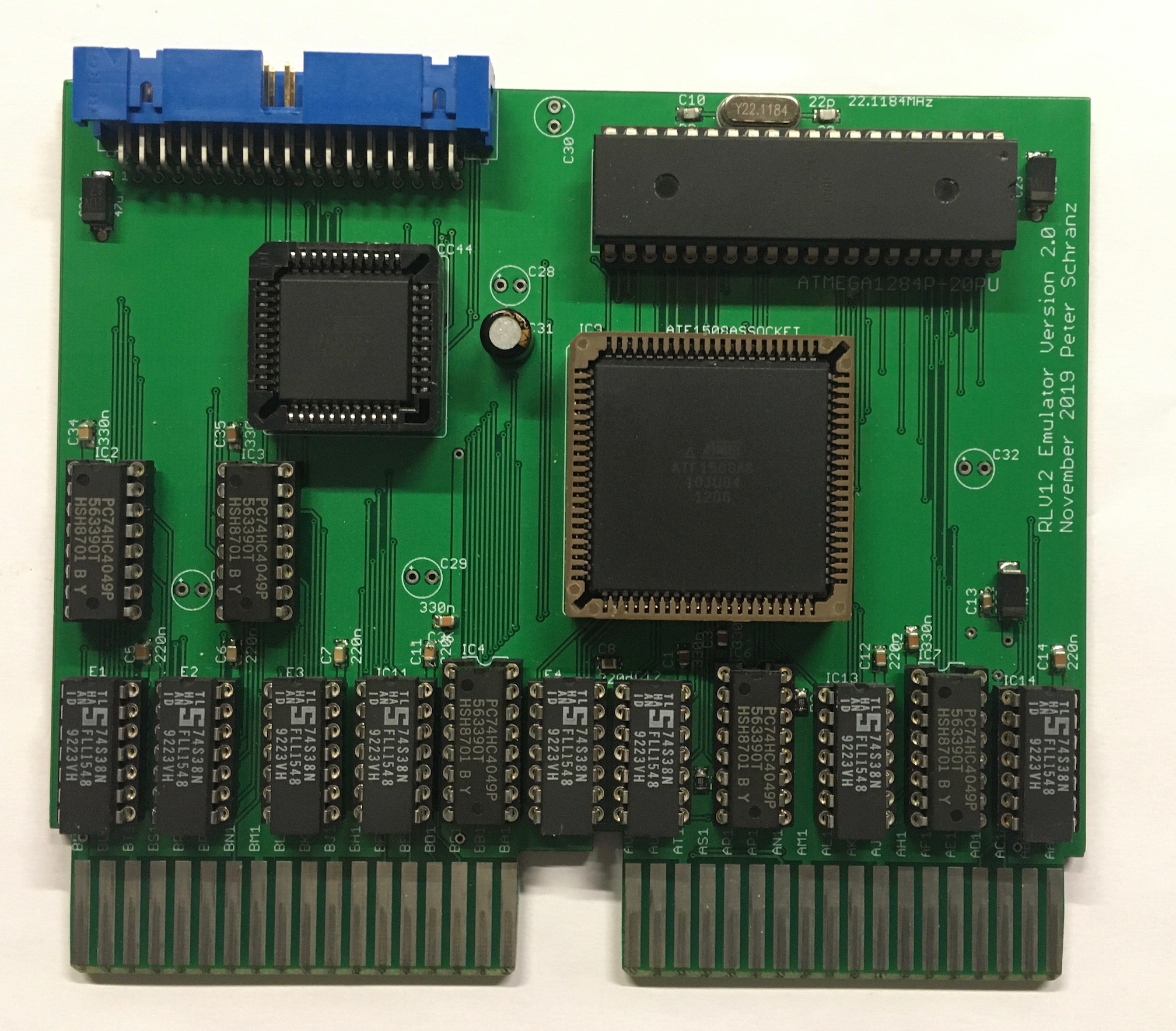
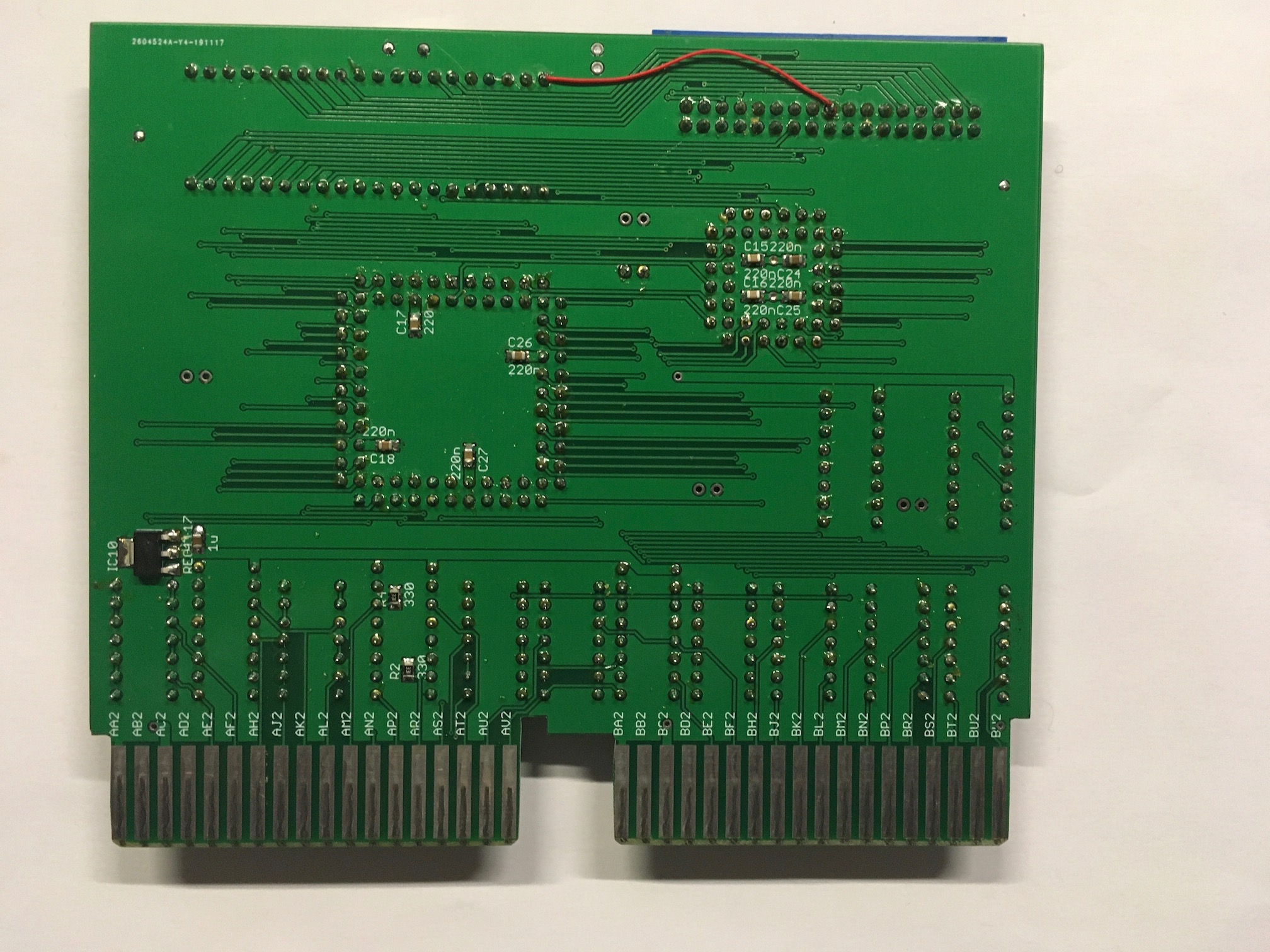
The bottom layer carries the 3V3 LDO regulator and some SMD capacitors. It is very important that only low-profile devices are soldered to the bottom side of the PCB. The specs for Q-Bus cards says no more than 1.6mm.
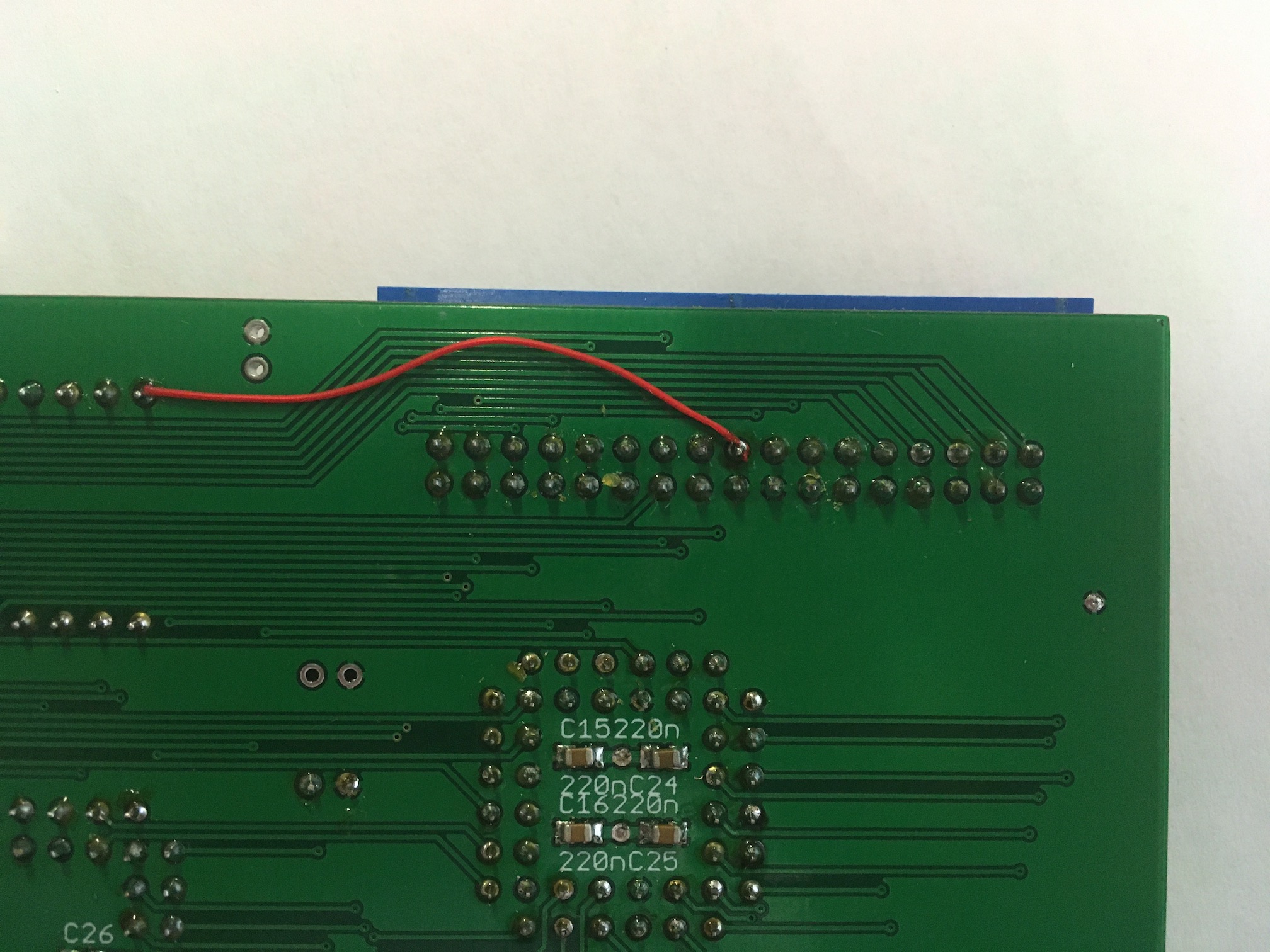
Activty LED
In order to have the activity LED you need to add a wire to the RLV12 Emulator V2.0 board. The wire goes from PIN 20 of the MCU to PIN 18 of the IDC-34 pin-header. You just need to add the wire, there are no other wires to cut, the correpsonding input of the CPLD is no longer active.
Programming the MCU
The break-out board has a standard Atmel ISP header to program the MCU. This is the 6-pin IDC header on the break-out board. Programming AVR MCUs can sometimes be confusing as there are several settings that must be correct. Also there are three areas that can/must be programmed.
The first challenge is when programming a new completely erased AVR microcontroller. In this state the internal 8MHz RC oscillator is activated from which the CPU clock is derived and in addition the system clock prescaler is activated and devides the RC clock by 8. So in fact the CPU is clocked only 1MHz. As the ISP clock rate must be no higher than ¼ of the CPU clock this means before you program the MCU you need to set the clock rate of the IPS programmer to be 250kHz or less. I always use a very low rate.
The first thing you should do is set the device type and check the signature. This is just to verify that we have inserted the correct MCU model into the emulator. In our case the device is a ATmega1248P
Once you have checked the correct signature you should program the fuses.
I normally use AVR Studio 4.19 to program my AVR microcontrollers. But to give you a better view of the required settings here a screenshot of AVRFuses
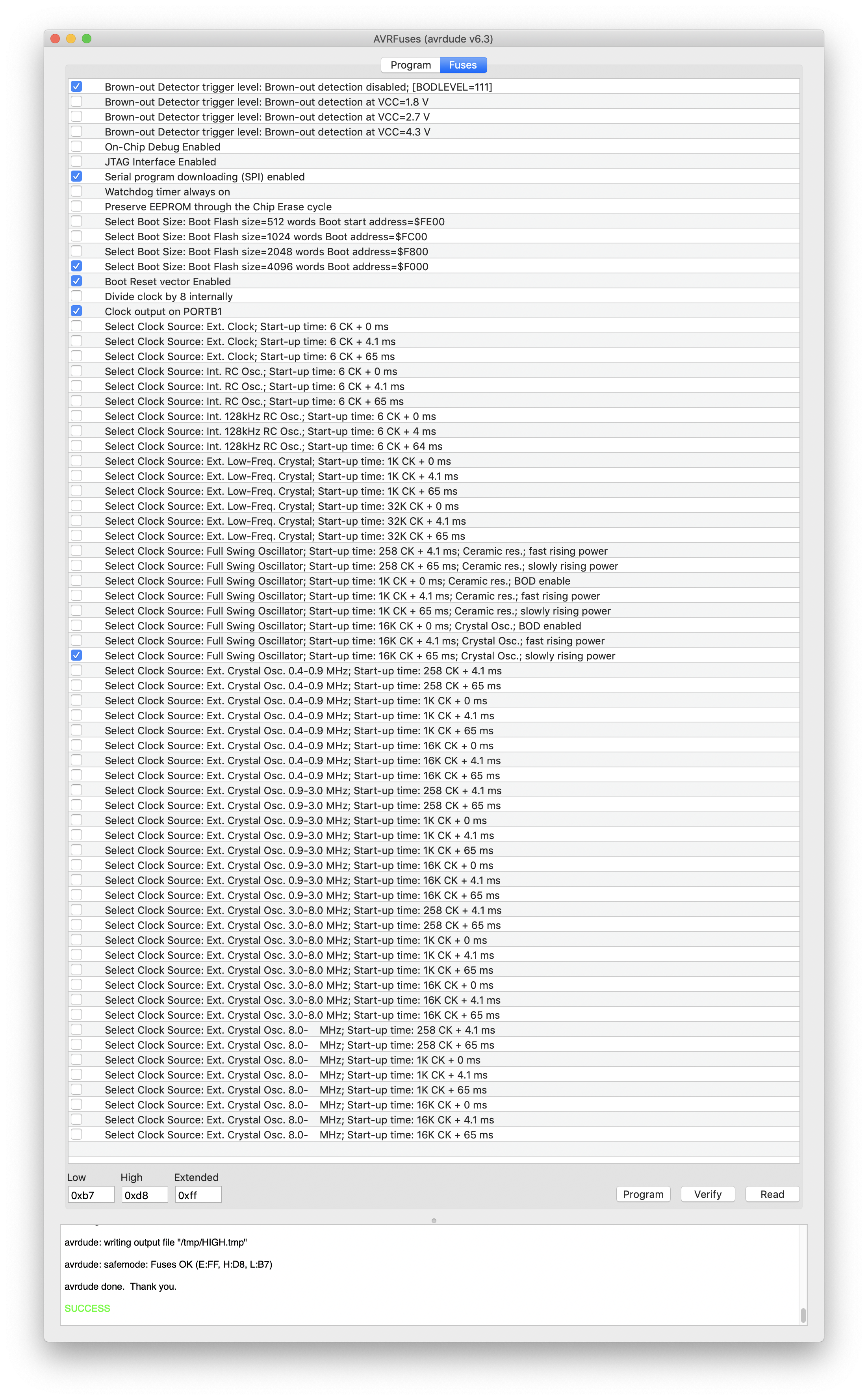
Make sure you have selected the same fuses as you can see in the picture. You can also use the hex values shown at the bottom of the screenshot.
It is very important that you disable the JTAG interface, disable the internal clock devide by 8, enable clock output on PB1 and enable the correct clock source. The option to output the system clock on PB1 is required as the CPLD uses the clock internally e.g. for the DMA statemachine.
Programming the CPLDs
This project includes two CPLDs. To program both CPLDs you need to know that they are daisy-chained via their respective JTAG interfaces. The JTAG interface is as well available on the break-out port and is the 10-in IDC header. The CPLDs can be programmed in-circuit via the JTAG interface. The ATF1504 is Chip 1 and the ATF1508 is Chip 2. You can find the necessary chain file in the download section.
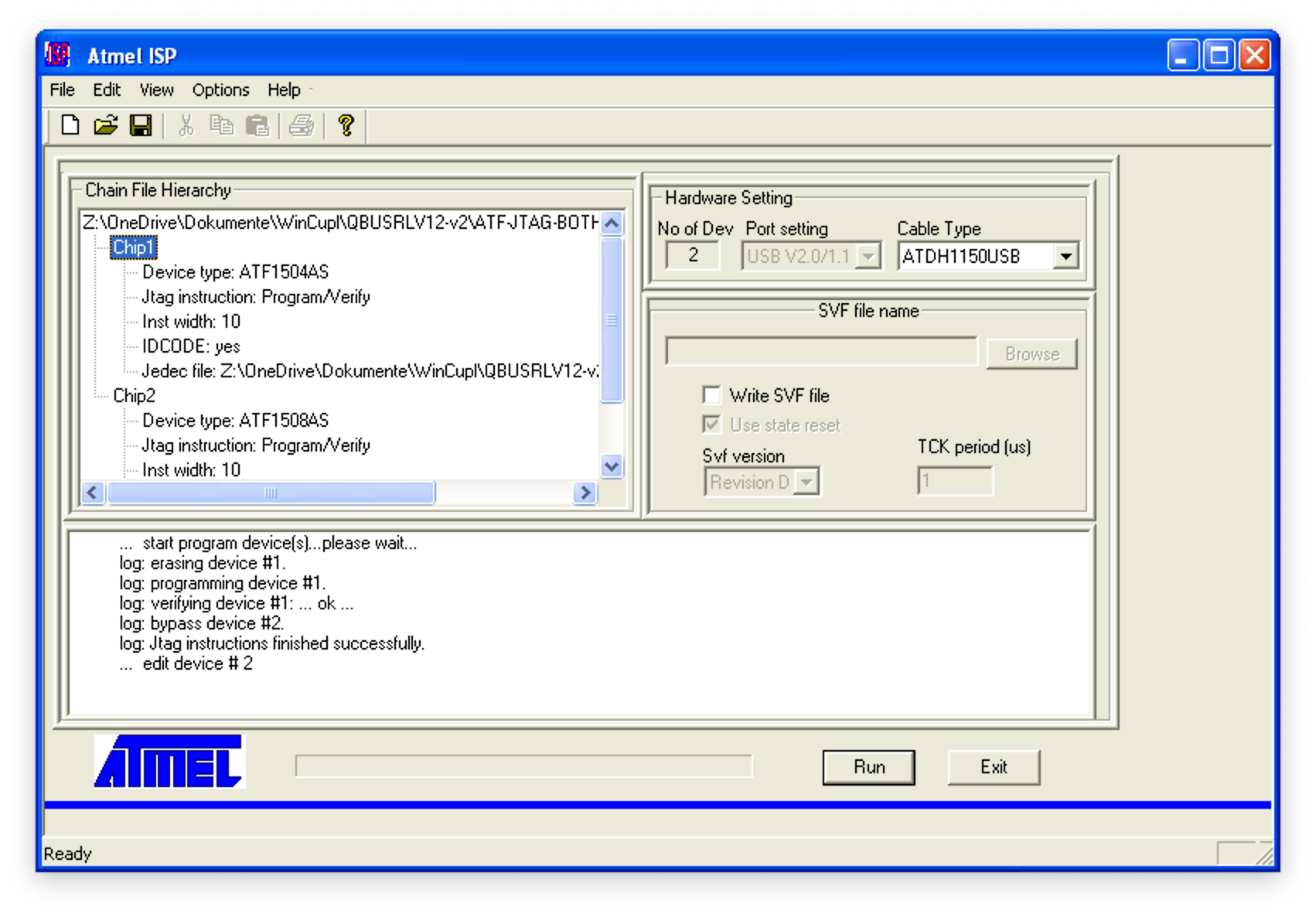
Unfortunately the program is a very old program no longer maintained and in Windows XP you cannot resize the sub-windows. So here just some words about the screenshot. First you see the main window which shows 2 chips. For each chip you need to set the JTAG instruction and the JEDEC file. Unfortunately the file name uses absolute paths, so in case you are using the chain file in the download section you need to adjust the files, by double-clicking on the filename.
You can of course create your own chain file, just select “New” in the “File”
menu. Set the number of chips to 2 and select the appropriate device type
and file. Make sure chip 1 is a ATF1504AS and chip 2 is a ATF1508AS. In case
you want to program the chips individually you can just use the Bypass
action of the chip you do not want to program.
Once you have setup everything hit the Run button. It takes quite some time
until you see a reaction and output on the lower part of the window. Be
patient.