RLV12 V2.0 Background
As mentioned the RLV12 Emulator V1.0 did come with some flaws that make it less easy to use. Most notably the programming interfaces for the AVR MCU (ISP) and the CPLD (JTAG) are virtually inaccessible when the card is plugged into a Q-Bus backplane. Also the SD-Card could not really be accessed from outside without using tweezers. And last but not least the console for the emulator required a special cable.
Another annoying fact is, that I used DS8837 Q-Bus receivers in a SOIC-16 SMD package which are very hard to find nowadays. I got some from China and they effectively were no fakes but I’m not very confident if this would always be the case.
As already shown with the Q-Bus memory it is possible to replace these with 74HC4049 operated at approx 3V3.
I also used a lot of SMD packages and especially the TQFP-100 package for the CPLD does not make it easy to build it for many that have no experience with SMD packages with a pitch of only 0.5mm.
Then I was also thinking about redesigning the DMA. V1.0 implemented a state machine that first requested the bus and when the DMA was granted informed the MCU. The MCU then transferred the data and signaled the state machine in the CPLD that the data transfer has been completed. Then the statemachine finished the DMA cycle. This process occupies the bus for more than would be necessary. However there were not enough resources in the CPLD for another 16-bit data register that could handle the data transfer. I already used a lot of resources for the address generation, address increment and the local copy of the CSR to avoid that the MCU is interrupted when the PDP-11 polls the CSR.
Therefore I decided to completely review the design and did the following changes:
-
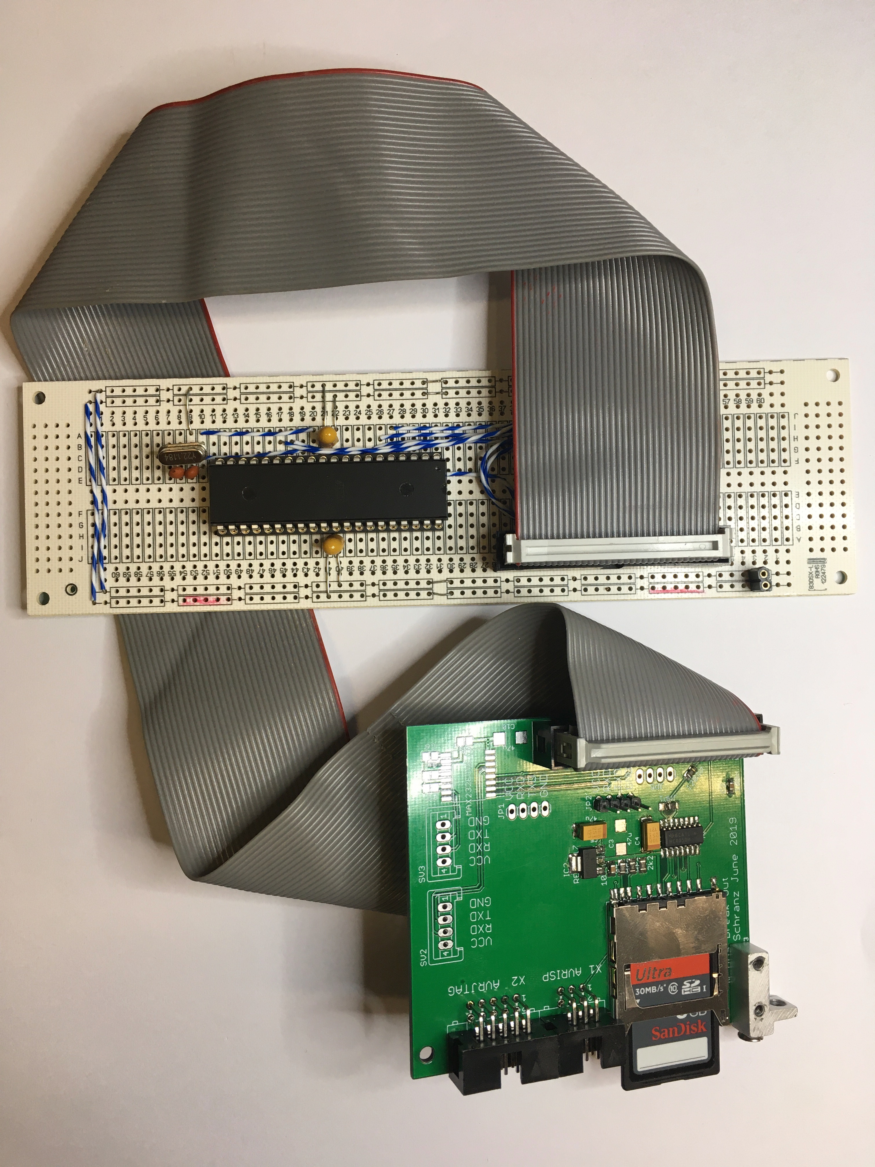
A single 34-pin IDC connector will carry all signals to an external break-out board. The break-out board has been designed so it could be mounted on a blind filler panel of a BA-23 case. It will carry the ISP, JTAG, the SD-Card and the serial interface to control the emulator. I finally managed to build a version of the SD-Card interface that would allow a 34-pin flat cable of approx 50cm, aka 20inches and still run the SPI to read/write the SD-Card at the maximum speed supported by the MCU
-
The 34-pin ribbon cable will be in some way a standardized interface to break-out boards in general, not only for the RLV12 Emulator but other projects I have in mind. E.g. it provides also free signals to carry more serial interfaces
-
All IC packages on the main-board are now through-hole packages with the exception of the 3V3 voltage regulator which comes in a SOT-223 package, which is very easy to solder by hand. Also I still prefer SMD resistors and capacitors as they are very cheap, small and still very easy to solder
-
There are no legacy Q-Bus Interface ICs. The Q-Bus interface is built using 74S38 open collector NAND gates and 74HC4049 buffer/inverters that are suited for high input voltage. Even when not operated at 5V or when not powered at all they accept an input voltage of up to 15V. These ICs are still in production and the same goes for the MCU and the CPLD, so no legacy parts.
-
By adding a small second CPLD to the design I have now enough resources for a dedicated DMA data register, so each DMA cycle is completely handled internally by the master CPLD. Each individual DMA cycle runs at the maximum speed the addressed RAM will allow. The DMA throughput itself will not increase but the time the DMA occupies the Q-Bus is somewhat reduced. Still the performance of the Emulator is much better than the real thing
The Break-Out Board
Here is a picture of the first break-out board version. This will in fact be the general standard break-out board for all of my ongoing designs, not only for the Q-Bus cards but as well for my PDP-11/Hack. Note the break-out is still all SMD because the SD-Card cages are only available as SMD parts, so it does not make sense to avoid other SMD parts with more or less the same difficulty to solder as the SD-Card cage. In addition SMD parts save a lot of sapce.
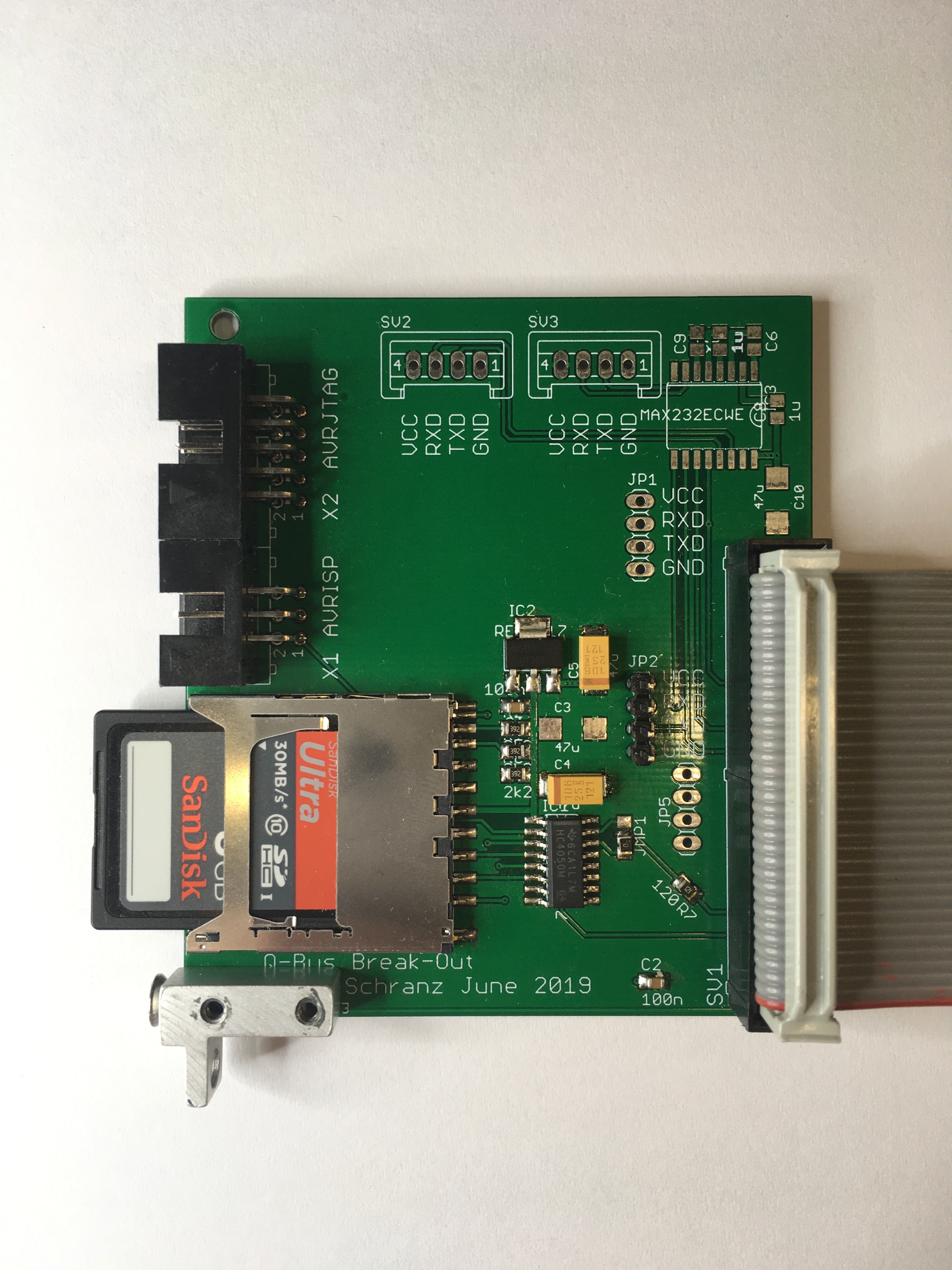
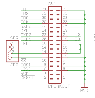
The layout of the 34-pin IDC is fixed and has dedicated signals for the ISP, JTAG and up to 4 serial interfaces. It also includes signals for CD (Card Detect) and WP (Write Protect) and 4 user defined signals. I intend to make this the standard break-out board for most of my designs.
Here you can see a picture of my test bed that was used to verify the maximum cable length and the operation of the JTAG and ISP interface. The MCU is the same as used on the RLV12 Emulator, a Atmega1284P, running at 22.1184MHz. I was using a modified firmware with no CPLD interface, but access to the SD-Card and the commands that can be used were the same.