RLV12 V2.0 Description
Schematic
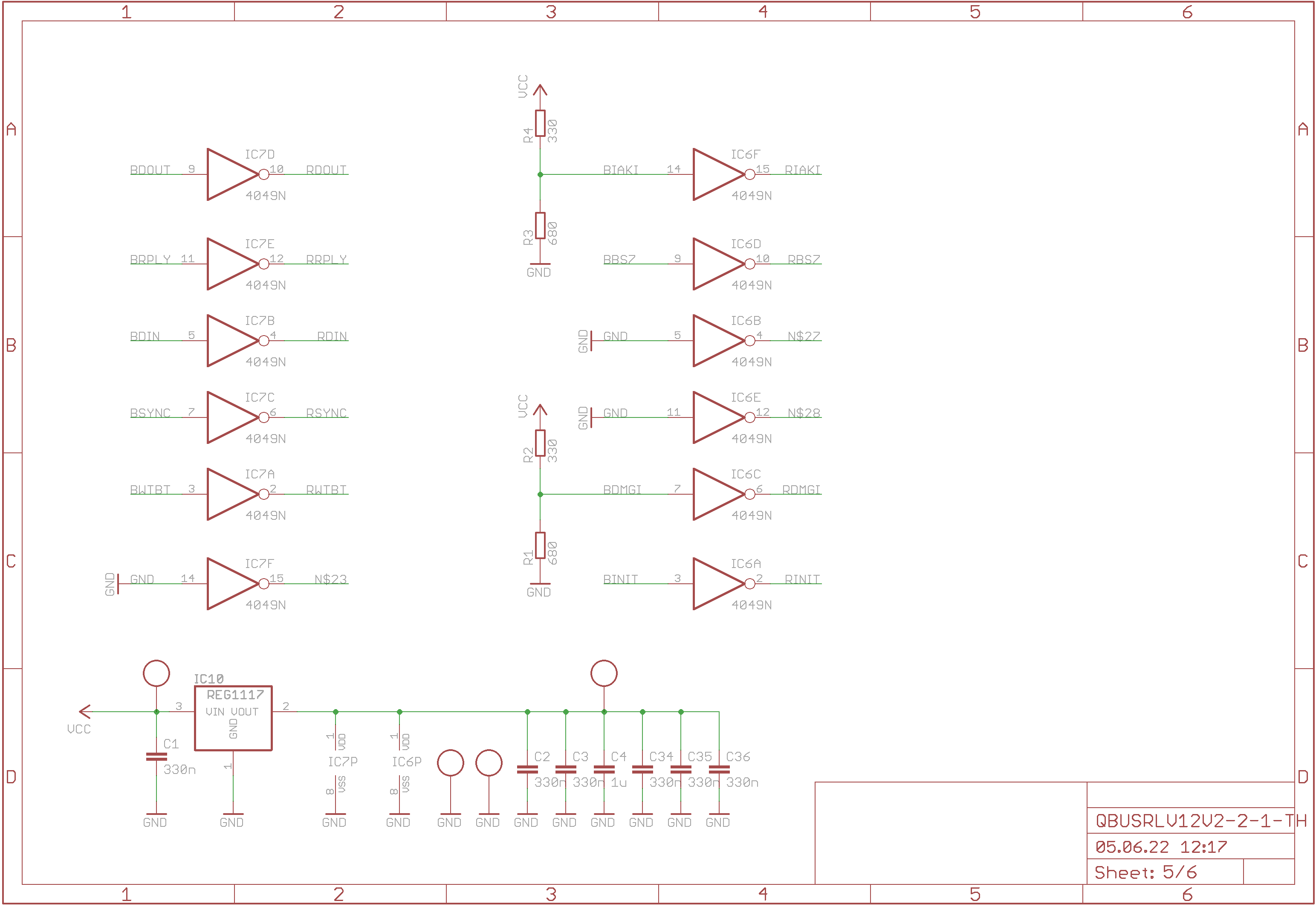
I have started to use the naming convention of digital, so the signals start either with B for Bus, R for Receive and T for Transmit and have an optional L at the end of the name if they are active low.
The first pages shows the section with the signals I receive from the Q-Bus. As already mentioned I’m using 74HC4049 and operate them with 3.3V. At this voltage the 74HC4049 have a threshold of approximatively 1.7V, which is the standard for Q-Bus receivers. I use a SMT LDO regulator in a SOT-23 package. I know that I said through hole only ICs but I think a SOT-23 is acceptable.
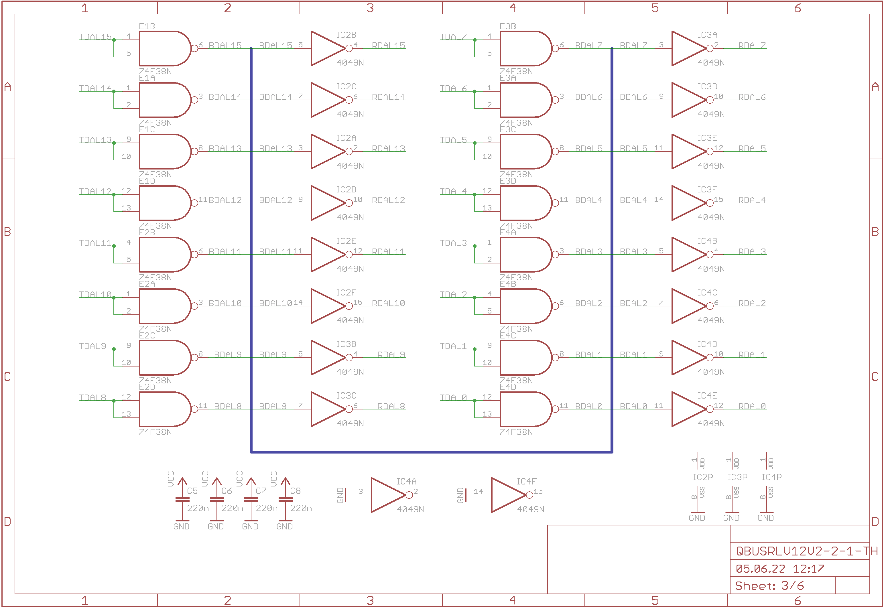
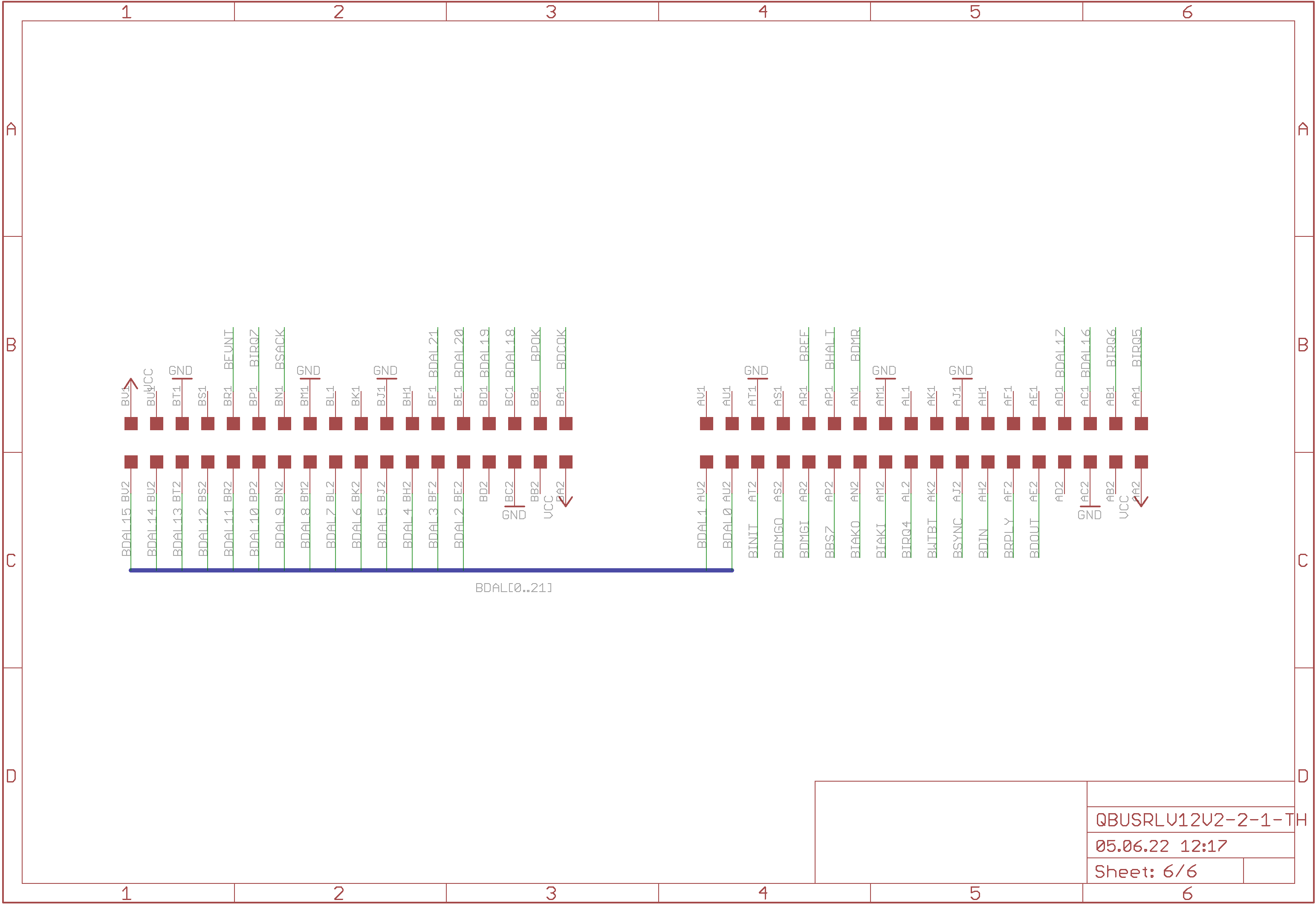
The next page shows the lower 16 bits of the multiplexed address/data bus. The Q-Bus is bidirectional but as I only use receivers and transmitters and no transceivers, like the DC005, I end with 16 bits receive and 16 bits transmit data signals.
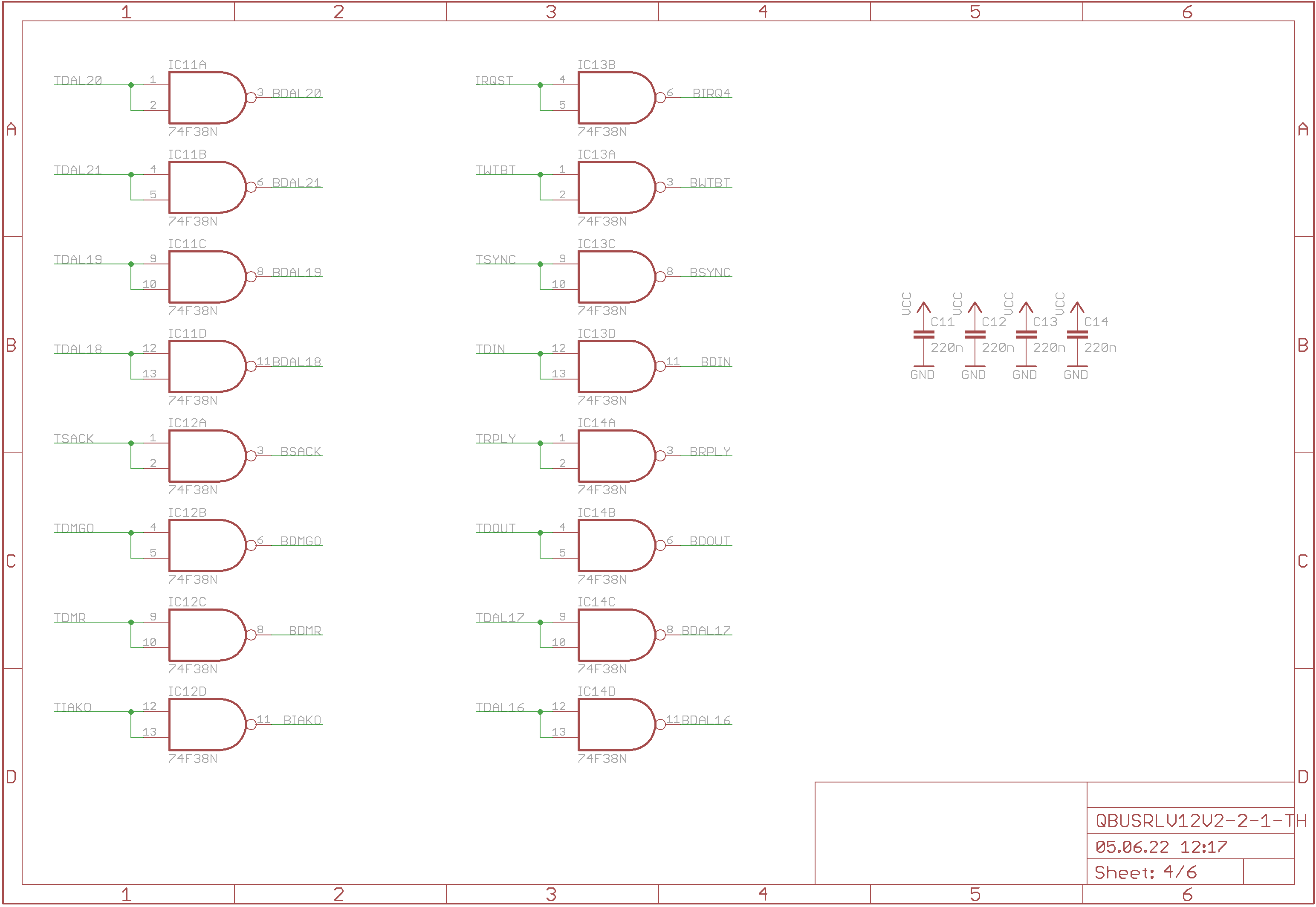
The next section shows the remaining signals I need to transmit to the Q-Bus. For each Q-Bus signal I need to be able to transmit and receive I end up with two signals the emulator has to interface with.
This is the reason I need a lot more PINs on the CPLD. Therefore I added a second
CPLD and divided the functions among the tow CPLDs. At the same time I tried to
avoid that a Q-Bus signal, receive or transmit, is being required by both CPLDs.
The only exceptions are RSYNC and RWTBT. Also only very few signals run
between the CPLDs themselves.
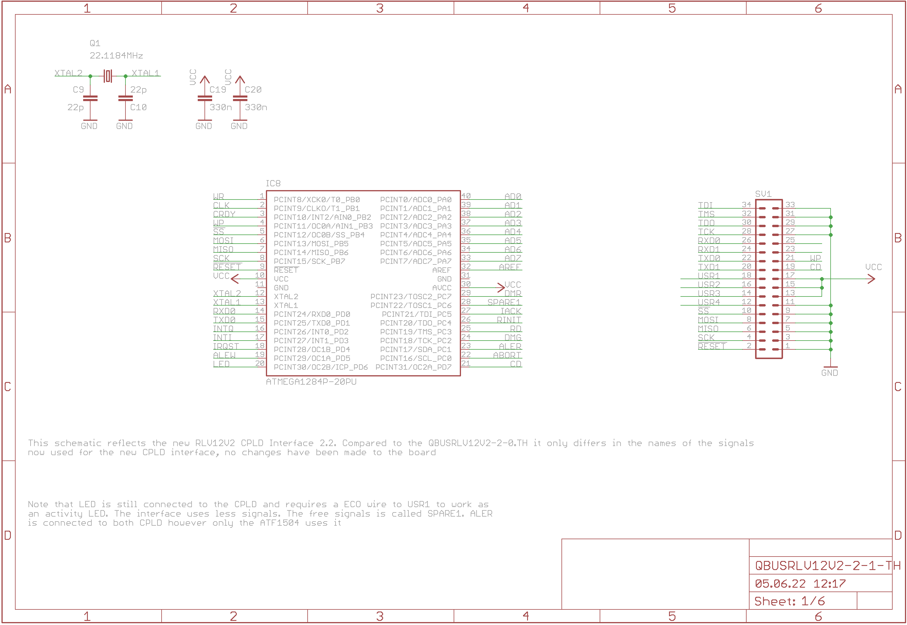
The rest of the schematic is very simple, there is the MCU and the IDC-34 connector for the ribbon cable that runs to the break-out board
and of course the Q-Bus interface
Function Blocks
The RLV12 Emulator consist of the following main functions
- Device register interface, whenever the PDP-11 reads or writes a device register the MCU is informed and processes the data.
- DMA State Machine
- Interrupt Logic for Interrupt Acknowledge Cycles
CPLD Functions
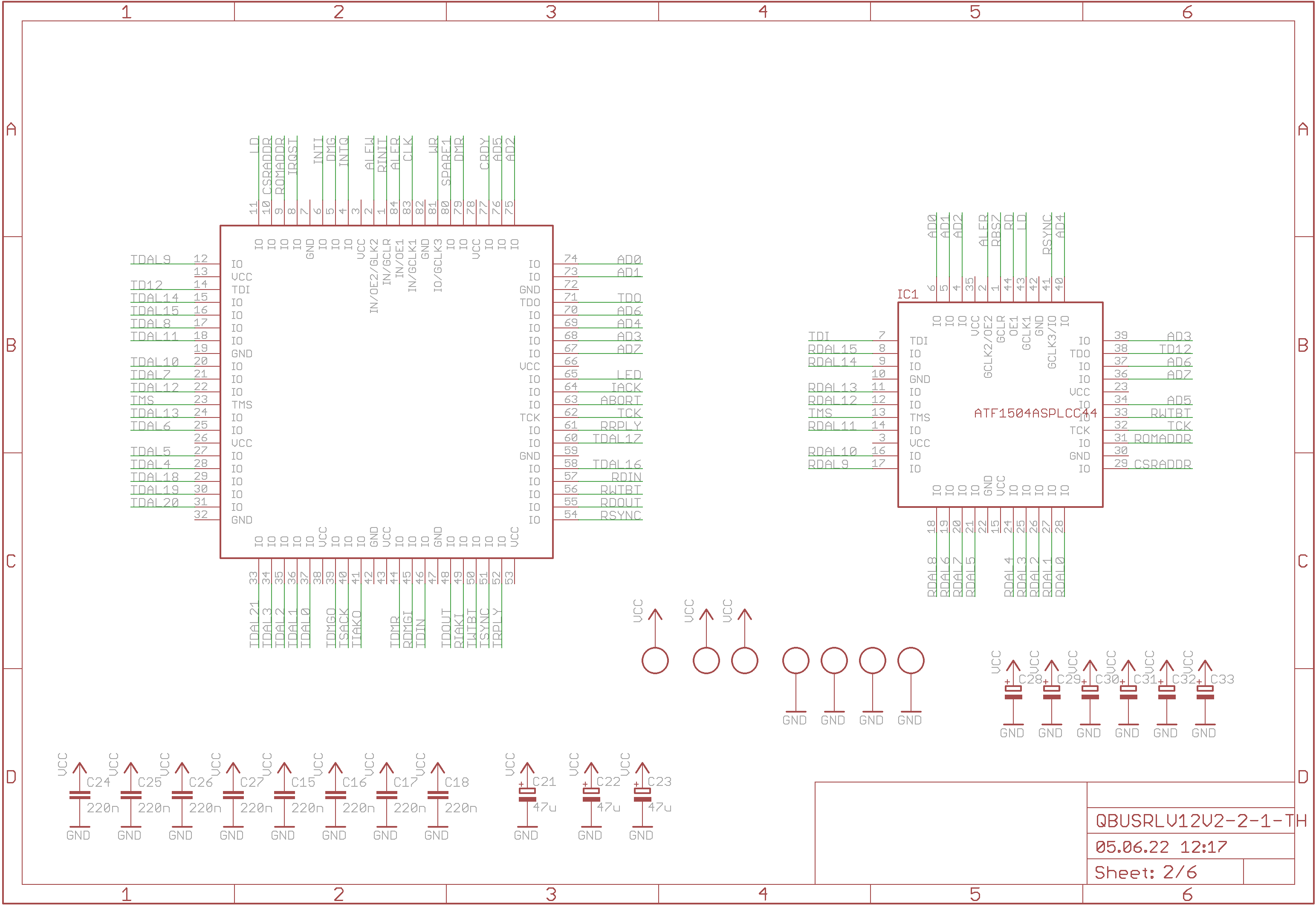
The GLUE logic has now been split into two CPLDs. The main CPLD still implements most of the functions that were used in the single CPLD of the RLV12 Emulator V1.0. To cover for the additional requirements regarding pins and registered resources the part that deals with reading the Q-Bus data/address has been moved to a second CPLD.
Main CPLD
The main CPLD is an ATF1508. It is very similar to the CPLD used on the first RLV12 Emulators except that it does not have any receive data register. The rest is pretty much identical.
As we have two CPLDs there are a few (in fact only 2) signals running between
them. The first signal is CSRADDR which is created by the receive CPLD and
signals that the a device register is being accessed.
The second signal LD is created by the DMA state machine of the main CPLD and
latches the DMA Read data into the DMA Read Register in the receive CPLD.
I have removed the CSR base register from the CPLD which results in a simpler bus interface logic and also avoids the conflict between the MCU updating the CSR and the PDP-11 reading the CSR. The downside is that the MCU is now interupted for every read access of the CSR even when the controller has set the busy bit. However the performance impact first only shows when the PDP-11 does polled IO.
The DMA state machine has changed slightly but works pretty much the same except it now signals the MCU when the DMA has finished and no longer signals the MCU that a data transfer is necessary. The handshaking using DMG is now used to let the MCU know when the DMA has finished.
Update 2020-10-18 RPLY for IACK cycles now waits for the MCU to finish the interrupt acknowledgement processing which is handled by an interrupt (INT2) service route in the MCU.
Name     QBUS RLV12 Version 2 ;
PartNo   A ;
Date     11.11.2019 ;
Revision 02 ;
Designer cbscpe ;
Company  PRIVAT ;
Assembly None ;
Location ATHOME ;
Device   f1508ispplcc84 ;


PIN		16	=  TDAL15;
PIN		15	=  TDAL14;
PIN		24	=  TDAL13;
PIN		22	=  TDAL12;
PIN		18	=  TDAL11;
PIN		20	=  TDAL10;
PIN		12	=  TDAL9;
PIN		17	=  TDAL8;
PIN		21	=  TDAL7;
PIN		25	=  TDAL6;
PIN		27	=  TDAL5;
PIN		28	=  TDAL4;
PIN		34	=  TDAL3;
PIN		35	=  TDAL2;
PIN		36	=  TDAL1;
PIN		37	=  TDAL0;

PIN		58	=  TDAL16;
PIN		60	=  TDAL17;

PIN		29	=  TDAL18;
PIN		30	=  TDAL19;
PIN		31	=  TDAL20;
PIN		33	=  TDAL21;

PIN		61	=  RRPLY;
PIN		57	=  RDIN;
PIN		55	=  RDOUT;
PIN		56	=  RWTBT;
PIN		54	=  RSYNC;
PIN		1	=  RINIT;
PIN		52	=  TRPLY;
PIN		46	=  TDIN;
PIN		48	=  TDOUT;
PIN		50	=  TWTBT;
PIN		51	=  TSYNC;
PIN		49	=  RIAKI;
PIN		41	=  TIAKO;
PIN		44	=  TDMR;
PIN		45	=  RDMGI;
PIN		39	=  TDMGO;
PIN		40	=  TSACK;

PIN		81	=  WRQ;		/* Dedicated Load for Q-Bus Data Reg.	*/
PIN		83	=  CLK;
PIN		2	=  WRD;		/* Dedicated Load for DMA Data Reg.	*/
PIN		80	=  WRA;		/* Dedicated Load for DMA Address Reg.	*/
PIN		74	=  AD0;
PIN		73	=  AD1;
PIN		75	=  AD2;
PIN		68	=  AD3;
PIN		69	=  AD4;
PIN		76	=  AD5;
PIN		70	=  AD6;
PIN		67	=  AD7;
PIN		8	=  IRQST;
PIN		79	=  DMR;
PIN		5	=  DMG;
PIN		4	=  INT0;
PIN		6	=  INT1;
PIN		77	=  INT2;
PIN		64	=  IACK;
PIN		63	=  ABORT;

PIN		10	=  CSRADDR;
PIN		11	=  LD;		/* Load Q-Bus to DMA Data Reg. CPLD B*/

/*
	!!!!!!!!!	This CPLD requires the interface '21' in the MCU firmware
	!!!!!!!!!	#define	rlv12	  21		; Select Assembler Option

 */
PROPERTY ATMEL {preassign KEEP};

PINNODE		=  [Q15..0]      ; /* Data Output Register			*/
PINNODE		=  [D15..0]      ; /* DMA Data Register				*/
PINNODE		=  [A21..1]      ; /* DMA Address				*/
PINNODE		=  [T7..0]       ; /* Temp Register for 16-bit writes		*/
PINNODE		=  CSR           ; /*						*/
PINNODE		=  [DMA4..0]     ; /* DMA State Machine				*/
PINNODE		=  SYNC          ; /*						*/
PINNODE		=  DMGI          ; /*						*/
PINNODE		=  SACK          ; /*						*/
PINNODE		=  DATA          ; /*						*/
PINNODE		=  RPLY          ; /*						*/
PINNODE		=  DMARW         ; /*  Control bit: DMA read(1) or DMA write(0)	*/
PINNODE		=  BUSEN         ; /*						*/
PINNODE		=  DIRQ          ; /* Device Interrupt Request			*/
PINNODE		=  DACK          ; /* Device Interrupt Acknowledge		*/
PINNODE		=  RECI          ; /*						*/

PINNODE		= [RS1..0];


/*
	Define one of the possible emulations: RLV12, RH70
 */
$DEFINE RLV12

/*
	Field definitions
 */
FIELD  RS       = [RS1..0];	/* Register Select Address for Atmega1281 reads/writes	*/
FIELD  DMA      = [DMA4..0];	/* DMA State Machine					*/
/*
	Register Select for DMA Address Registers
 */

RS.ar		=  ABORT;
RS.ck		= !WRA;
RS0.t		= 'b'1;
RS1.t		= RS0;

CSR.ck		=  RSYNC;
CSR.d		=  CSRADDR;

/*
	The device registers are effectively implemented within the MCU.
	When the PDP-11 accesses a device register the MCU is interrupted
	and must either read the value from the Q-Bus (DATO/DATOB) or
	write the requested register content to the Q-Bus data register.
	At the same time the MCU must perform all processing that must be
	performed immediately. When the MCU has finished processing the
	device register IO it has to acknowledge the interrupt using the
	IACK signal (i.e. create a short pulse on IACK). The CPLD will then
	assert RPLY to signal the PDP-11 to proceed. Note that all processing
	of the MCU must be done within the Q-bus-timeout, which is about 10usec.


	DATI to a device register triggers INT1 interrupt of the MCU.
 */
INT1.d		= !(!RWTBT &  CSRADDR);
INT1.ck		=  RSYNC;
INT1.ap		=  IACK;

/*
	DATO/DATOB to a device register triggers INT0 interrupt of the MCU.
 */
INT0.d		=  !(RWTBT &  CSRADDR);
INT0.ck		=  RSYNC;
INT0.ap		=  IACK;

TRPLY		=  CSR &  RSYNC &  INT1 &  RDIN		/* Assert RPLY when MCU is done	*/
		#  CSR &  RSYNC &  INT0 &  RDOUT;	/* Assert RPLY when MCU is done	*/

/*
	The interrupt logic is now fully handled in software so we can also
	update any register if needed. The CPU sets IRQST whenever an interrupt is
	required. This asserts !BIRQ on the QBUS. The PDP-11 will then perform an
	interrupt acknowledge cycle. That is it will assert BDIN without asserting
	BSYNC previously. This is because BDIN is used by all devices to freeze the
	interrupt request status in an internal register. After BDIN the PDP-11
	will assert BIAKO of the CPU board. BIAKO of each slot is connected to
	BIAKI of the next slot building a daisy chain. Each device needs to
	monitor BIAKI and in case it is not requesting the interrupt it must
	assert BIAKO. This decision is made by every card at the same time
	using the latched interrupt request status (DACK). The first device
	with DACK being asserted must not assert BIAKO but instead must place
	the interrupt vector onto the bus and assert BRPLY and de-assert
	the interrupt request. The PDP-11 will then read the vector from
	the bus and de-assert BIAKO and BDIN and the device must remove the
	vector data from the bus.

	If BIAKI is asserted and we have requested an interrupt this now triggers
	INT2 interrupt of the MCU. The MCU must then de-assert IRQST and assert
	the interrupt using IACK. At the same time it can do some  post interrupt
	processing. E.g. the IE of the CSR of a RH70 is automatically cleared
	when an interrupt is acknowledged. This could also be used to implement
	a programmable interrupt vector.

	In the case of the RLV12 the MCU only needs to clear the IRQST signal
	and acknowledge the interrupt using IACK.

 */
DACK.d		=  IRQST;
DACK.ck		=  RDIN;
DACK.ar		=  RINIT;

TIAKO		=  RIAKI & !DACK;
/*TIRQ		=  IRQST;*/

INT2.d		= !DACK;
INT2.ck		=  RIAKI;
INT2.ap		=  IACK;

APPEND
TRPLY		=  RIAKI & RDIN & DACK & INT2;

/*
	DMA Data Register
 */
[D7..0].d	=  [AD7..0];
[D15..8].d	=  [D7..0];
[D15..0].ck	=  WRD;

/*
	Q-Bus Data Register
 */
[Q7..0].d	=  [AD7..0];
[Q15..8].d	=  [Q7..0];
[Q15..0].ck	=  WRQ;

/*
	DMA Address
 */
DMARW.ar	=  WRA &  RS:['d'0] & !AD0;
DMARW.ap	=  WRA &  RS:['d'0] &  AD0;
DMARW.ck	= 'b'0;
DMARW.d		= 'b'0;

[A7..1].ar	=  WRA &  RS:['d'0] & ![AD7..1];
[A7..1].ap	=  WRA &  RS:['d'0] &  [AD7..1];

[A15..8].ar	=  WRA &  RS:['d'1] & ![AD7..0];
[A15..8].ap	=  WRA &  RS:['d'1] &  [AD7..0];

[A21..16].ar	=  WRA &  RS:['d'2] & ![AD5..0];
[A21..16].ap	=  WRA &  RS:['d'2] &  [AD5..0];

/*
	Synchronous counter for DMA address which is updated after every DMA
	cycle. The address is incremented whenever a DMA cycle has finished.
 */
[A21..1].ck	= !DMR;

A1.t		= 'b'1;
A2.t		= A1;
A3.t		= A1 & A2;
A4.t		= A1 & A2 & A3;
A5.t		= A1 & A2 & A3 & A4;
A6.t		= A1 & A2 & A3 & A4 & A5;
A7.t		= A1 & A2 & A3 & A4 & A5 & A6;
A8.t		= A1 & A2 & A3 & A4 & A5 & A6 & A7;
A9.t		= A1 & A2 & A3 & A4 & A5 & A6 & A7 & A8;
A10.t		= A1 & A2 & A3 & A4 & A5 & A6 & A7 & A8 & A9;
A11.t		= A1 & A2 & A3 & A4 & A5 & A6 & A7 & A8 & A9 & A10;
A12.t		= A1 & A2 & A3 & A4 & A5 & A6 & A7 & A8 & A9 & A10 & A11;
A13.t		= A1 & A2 & A3 & A4 & A5 & A6 & A7 & A8 & A9 & A10 & A11 & A12;
A14.t		= A1 & A2 & A3 & A4 & A5 & A6 & A7 & A8 & A9 & A10 & A11 & A12 & A13;
A15.t		= A1 & A2 & A3 & A4 & A5 & A6 & A7 & A8 & A9 & A10 & A11 & A12 & A13 & A14;
A16.t		= A1 & A2 & A3 & A4 & A5 & A6 & A7 & A8 & A9 & A10 & A11 & A12 & A13 & A14 & A15;
A17.t		= A1 & A2 & A3 & A4 & A5 & A6 & A7 & A8 & A9 & A10 & A11 & A12 & A13 & A14 & A15 & A16;
A18.t		= A1 & A2 & A3 & A4 & A5 & A6 & A7 & A8 & A9 & A10 & A11 & A12 & A13 & A14 & A15 & A16 & A17;
A19.t		= A1 & A2 & A3 & A4 & A5 & A6 & A7 & A8 & A9 & A10 & A11 & A12 & A13 & A14 & A15 & A16 & A17 & A18;
A20.t		= A1 & A2 & A3 & A4 & A5 & A6 & A7 & A8 & A9 & A10 & A11 & A12 & A13 & A14 & A15 & A16 & A17 & A18 & A19;
A21.t		= A1 & A2 & A3 & A4 & A5 & A6 & A7 & A8 & A9 & A10 & A11 & A12 & A13 & A14 & A15 & A16 & A17 & A18 & A19 & A20;

/*
	Q-Bus Output Select and Output Enable

	DMA4	DMA Read is active
	DMA3	DMA is active
	DMA2	DMA data transfer
 */
[TDAL15..0]	= !RIAKI &           DMA3  & !DMA2  &  [A15..1, 'b'0]
		# !RIAKI & !DMA4  &  DMA3  &  DMA2  &  [D15..0]
		# !RIAKI & !DMA3  &  CSR   &  RDIN  &  [Q15..0]

$IFDEF RLV12
		#  RIAKI          &  DACK  &  RDIN  &  'o'160;
$ENDIF
$IFDEF RH70
		#  RIAKI          &  DACK  &  RDIN  &  'o'254;
$ENDIF

/*
	The upper address bits are just a copy of the DMA address.
 */
[TDAL21..16]	=  [A21..16] &  DMA3  & !DMA2;

 /*
 	The rising edge of DMR from the MCU triggers BDMR of the Q-Bus when
 	the DMA is granted BDMR is cleared but DMR will be kept asserted by
 	the MCU until the MCU has finished the DMA. Used to control the state
 	machine.
  */
TDMR.d		= 'b'1;
TDMR.ck		=  DMR;
TDMR.ar		=  DMA3 # RINIT # ABORT;

TSYNC.ck	=  CLK;
TDOUT.ck	=  CLK;
TDIN.ck		=  CLK;
/*
	Synchronous Signals
 */
DMGI.ck		=  CLK;
DMA.ck		=  CLK;
RPLY.ck		=  CLK;
DMG.ck		=  CLK;
LD.ck		=  CLK;

DMA.ar		=  RINIT # ABORT;
 /*
 	Latched BDMGI and BRPLY as we need a stable DMGI and RPLY for the state machine
  */
DMGI.d		=  RDMGI;
RPLY.d		=  RRPLY;

/*
	For DMA writes the MCU must first load the DMA data register. Then it
	sets DMR which asserts BDMR. Then eventually the statemachine proceeds
	to state 'h'8 places the DMA address, asserts TSYNC, asserts TDOUT and
	waits for RPLY and then finishes the cycle.

	For DMA reads the MCU just sets DMR which asserts BDMR. The state
	machine proceeeds to stae 'h'18, places the DMA address, asserts
	TSYNC, asserts TDIN and waits for RPLY and then finishes the cycle.
	After that the MCU can read the DMA data register.
 */
sequence DMA {

   PRESENT 'h'00 IF !DMGI                    NEXT 'h'00;
                 IF  DMGI                    NEXT 'h'01;

   PRESENT 'h'01 IF !DMR                     NEXT 'h'02;
                 IF  DMR                     NEXT 'h'03;

   PRESENT 'h'02 IF !DMGI                    NEXT 'h'00;
                 IF  DMGI OUT TDMGO;         NEXT 'h'02;

   PRESENT 'h'03 IF !DMARW                   NEXT 'h'08;
                 IF  DMARW                   NEXT 'h'18;

/*
     DMG

     At the end of the DMA cycle the state machine asserts DMG to let the MCU
     know that the DMA has ended. The MCU then must de-assert DMR before it can
     start another DMA. This is placed to a state with TSACK de-asserted to
     release the bus while we are waiting for the MCU.

*/

   PRESENT 'h'04 IF  DMR                     NEXT 'h'04           OUT DMG;
                 IF !DMR                     NEXT 'h'00;
/*
     Write
*/
   PRESENT 'h'08                             NEXT 'h'09;

   PRESENT 'h'09                             NEXT 'h'0A OUT TSYNC;

   PRESENT 'h'0A                             NEXT 'h'0B OUT TSYNC;

   PRESENT 'h'0B                             NEXT 'h'0C OUT TSYNC OUT TDOUT;

   PRESENT 'h'0C IF !RPLY                    NEXT 'h'0C OUT TSYNC OUT TDOUT;
                 IF  RPLY                    NEXT 'h'0D OUT TSYNC OUT TDOUT;

   PRESENT 'h'0D                             NEXT 'h'0E OUT TSYNC OUT TDOUT;
   PRESENT 'h'0E IF  RPLY                    NEXT 'h'0E OUT TSYNC;
                 IF !RPLY                    NEXT 'h'0F;

   PRESENT 'h'0F                             NEXT 'h'04           OUT DMG;

/*
     Read
*/
   PRESENT 'h'18                             NEXT 'h'19;

   PRESENT 'h'19                             NEXT 'h'1A OUT TSYNC;

   PRESENT 'h'1A                             NEXT 'h'1B OUT TSYNC;

   PRESENT 'h'1B                             NEXT 'h'1C OUT TSYNC OUT TDIN OUT LD;

   PRESENT 'h'1C IF !RPLY                    NEXT 'h'1C OUT TSYNC OUT TDIN OUT LD;
                 IF  RPLY                    NEXT 'h'1D OUT TSYNC OUT TDIN OUT LD;

   PRESENT 'h'1D                             NEXT 'h'1E OUT TSYNC OUT TDIN OUT LD;

   PRESENT 'h'1E IF  RPLY                    NEXT 'h'1E OUT TSYNC;
                 IF !RPLY                    NEXT 'h'1F;

   PRESENT 'h'1F                             NEXT 'h'04           OUT DMG;
}

TSACK		=          DMA3;
TWTBT		= !DMA4 &  DMA3 & !DMA2;
Second CPLD
The logic of the second CPLD is rather simple and there are not many comments. The
only speciality is the internal register select register which can be loaded with
any register address and at the same time implements a read sequence. So when you
first have to read the device register address and then the Q-Bus for DATO/DATOB
cycle it is sufficient to load the register select with address zero and then
read three bytes. The same is true for the DMA Read data register. You first load
the register address one and then perform two reads to retrieve the low and the
high byte.
The ATF1504 deals primarily with the receive side of the address/data bus and implements the following functions.
First it latches the lower address bits that identify the device register
being selected. It also generates the CSRADDR signal to inform the main
CPLD that a device register is being addressed.
PINNODE 	        = [C5..0]       ; /* CSR Address					*/

FIELD  ADDR     	= [C5..0];	/* Latched address used for register address		*/
FIELD  RS       	= [RS2..0];	/* Register Select Address for Atmega1281 reads/writes	*/
FIELD  IOADDR   	= [RDAL12..0];	/* Access to IO Page only requires address lines 0..12	*/

/*
	Device Address is also generated by this CPLD as only we see the address
 */
ADDR.d			=  [RDAL5..0];
ADDR.ck			=  RSYNC;

/*
	CSR Select must be generated in this CPLD as we are the only CPLD that receives
	the DAL status from the BUS
 */
CSRADDR			=  RBS7 &  IOADDR:['o'174400..174417];
The DMA Read Data Register. Remember this CPLD is the only one that can read data
from the Q-Bus. Therefore there is a DMA Read Data register that latches the
data from the Q-Bus during DMA Read. The LD signal is created by the DMA
statemachine of the main CPLD.
[Q15..0].l		= [RDAL15..0];
[Q15..0].le		=  LD;
MCU Interface Control Interface is implemented as a register select address and a state machine. The MCU can address the five readable register individually. But it can also access them sequentially. There are two sequences typically required. The first is the sequence is used for DATO/DATOB cycles
- Device Register Address
- Q-Bus data low byte
- Q-Bus data high byte
and the second sequence is used to read the DMA Read data register
- DMA Read data low byte
- DMA Read data high byte
Adding a statemachine to the register select address increases the performance of the interface between the CPLD and the MCU. The MCU has no external memory interface which would make all this obsolete. But there is no high-speed AVR processor (≥20MHz) with enough RAM (≥8kbyte)
RS.ar			= ![AD2..0].io & ALE & !RD;
RS.ap			=  [AD2..0].io & ALE & !RD;
RS.ce			=  RD;
RS.ck			=  ALE;

sequence RS {

	present 'd'0	next 'd'2;

	present 'd'1	next 'd'3;

	present 'd'2	next 'd'4;

	present 'd'3	next 'd'5;

	present 'd'4	next 'd'0;

	present 'd'5	next 'd'0;
}
The MCU Data Interface provides 5 registers the MCU can read. Note how the device address register encodes which byte is being read and how the address bits are shuffled to make the lower 5 bits a direct index into a AVR MCU jump table without the need to shift bits. In addition the two signals UB and LB that inform the MCU whether the upper or lower byte are written by a DATO/DATOB cycle are now inverted. This reduces the number of product terms requried for AD6 and AD7 by the optimization algorithm of WinCUPL.
The other four registers are used to read the Q-Bus and the DMA Read data register.
UB			= !RWTBT
			#  RWTBT  &  C0;
LB			= !RWTBT
			#  RWTBT  & !C0;

[AD7..0]		=  RS:['d'2] &  [RDAL7..0].io
			#  RS:['d'4] &  [RDAL15..8].io
			#  RS:['d'1] &  [Q7..0]
			#  RS:['d'3] &  [Q15..8]
			#  RS:['d'0] &  [!UB, !LB, C0, C5, C4, C3, C2, C1];

[AD7..0].oe		=  RD;
The following is the complete CPLD design file of the second CPLD. Separating
the receive data bus form the rest of the logic provides a very efficient
usage of CPLD pins. The number of available pins has always been an issue in
many of my projects. The only common input signals of the two CPLDs are
RWTBT and RSYNC and the only signals that run between the two CPLDs are
CSRADDR and LD.
Name     QBUS RLV12 Version 2 ;
PartNo   B ;
Date     24.09.2019 ;
Revision 02 ;
Designer cbscpe ;
Company  PRIVAT ;
Assembly None ;
Location ATHOME ;
Device   f1504ispplcc44 ;


/*
	Second CPLD which only performs read of the data bus there are 5 registers
	that can be read

	Device Address		This is a copy of A1..5 latched with each SYNC together
				with two bits, UB and LB, that combine WTBT with A0 which
				are reset if the respective byte should be updated
				for DATOB cycles. They are reset for DATO cycles
	Q-Bus Data		These two register provide the current status of the
				lower 16-bits of the multiplexed address/data bus and
				are used to read the data in a DATO/DATOB cycle
	DMA Data		This 16-bit register will store the data of a DMA read
				cycle

	You can read the registers sequentially

	Device Address(0) -> Q-Bus Low(2) -> Q-Bus High(4)
	and
	DMA Data Low(1) -> DMA Data High(3)

	When RD is reset then ALE just loads the register select. If RD is high ALE
	selects the next register in sequence. So typically you only need to set
	the register select either to 0x00 or 0x01 and then you can just select the
	next register by creating a pulse on ALE.
	When RD is set then the output of the AD multiplexor is enabled and you can
	read the content of the selected register.
	2018-12-08
	-	Remove CS1ADDR no longer required after we removed CSR from CPDL A

	!!!!!!!!!	This CPLD requires the interface '21' in the MCU firmware
	!!!!!!!!!	#define	rlv12	  21		; Select Assembler Option

 */
PIN	28	=  RDAL0;
PIN	27	=  RDAL1;
PIN	26	=  RDAL2;
PIN	25	=  RDAL3;
PIN	24	=  RDAL4;
PIN	21	=  RDAL5;
PIN	19	=  RDAL6;
PIN	20	=  RDAL7;
PIN	18	=  RDAL8;
PIN	17	=  RDAL9;
PIN	16	=  RDAL10;
PIN	14	=  RDAL11;
PIN	12	=  RDAL12;
PIN	11	=  RDAL13;
PIN	9	=  RDAL14;
PIN	8	=  RDAL15;
PIN	6	=  AD0;
PIN	5	=  AD1;
PIN	4	=  AD2;
PIN	39	=  AD3;
PIN	40	=  AD4;
PIN	34	=  AD5;
PIN	37	=  AD6;
PIN	36	=  AD7;
PIN	41	=  RSYNC;
PIN	33	=  RWTBT;
PIN	1	=  RBS7;
PIN	29	=  CSRADDR;
PIN	43	=  LD;
PIN	44	=  RD;
PIN	2	=  ALE;

PROPERTY ATMEL {preassign=KEEP};
PROPERTY ATMEL {CASCADE_LOGIC=ON};
PROPERTY SOFT_BUFFER {UB, LB};

PINNODE		= [Q15..0];
PINNODE		= [RS2..0];
PINNODE         = [C9..0] ;	/* CSR Address						*/

FIELD  ADDR    	= [C9..0];	/* Latched address used for register address		*/
FIELD  RS      	= [RS2..0];	/* Register Select Address for Atmega1281 reads/writes	*/
FIELD  IOADDR  	= [RDAL12..0];	/* Access to IO Page only requires address lines 0..12	*/

/*
	Device Address is also generated by this CPLD as only we see the address
 */
ADDR.d		= [RDAL9..0];
ADDR.ck		=  RSYNC;

/*
	CSR Select must be generated in this CPLD as we are the only CPLD that receives
	the DAL status from the BUS
 */
CSRADDR		=  RBS7 &  IOADDR:['o'174400..174417];

/*
	DMA Data Register for DMA reads
 */
[Q15..0].l	= [RDAL15..0];
[Q15..0].le	=  LD;

/*
	Register Select we support two sequences

	0->2->4		to read the Device Address, followed by the Q-Bus
	1->3->5		to read the DMA data register (5 is not used)
 */
RS.ar		= ![AD2..0].io & ALE & !RD;
RS.ap		=  [AD2..0].io & ALE & !RD;
RS.ce		=  RD;
RS.ck		=  ALE;

sequence RS {

	present 'd'0	next 'd'2;

	present 'd'1	next 'd'3;

	present 'd'2	next 'd'4;

	present 'd'3	next 'd'5;

	present 'd'4	next 'd'0;

	present 'd'5	next 'd'0;
}

UB			= !C9 & !RWTBT
			# !C9 &  RWTBT  &  C0
			#  C9 & !C8;
LB			= !C9 & !RWTBT
			# !C9 &  RWTBT  & !C0
			#  C9 & !C7;

[AD7..0]		=  RS:['d'2] &  [RDAL7..0].io
			#  RS:['d'4] &  [RDAL15..8].io
			#  RS:['d'1] &  [Q7..0]
			#  RS:['d'3] &  [Q15..8]
			#  RS:['d'0] &  [!UB, !LB, C6, C5, C4, C3, C2, C1];

[AD7..0].oe		=  RD;
When placing signals ot the PINs you need to pay special attention to the
RD and the ALEsignal so they are using one of the global output enable
or clock signals. By using a global output enable input for RD the output
enable term is not using a macro-cell product-term so a single macro-cell
can be used as a 5-to-1 multiplexor, perfect for the 5 byte registers to read.
The second important point is that ALE is using one of the global clock inputs
because only then you can use the clock enable input of a macro-cell.
MCU Firmware
The MCU Firmware is the same for all RLV12 Emulator versions. There is now an assembler option to select the appropriate hardware. So all Emulators provide the same features.