RLV12 Emulator Schematic
Schematic
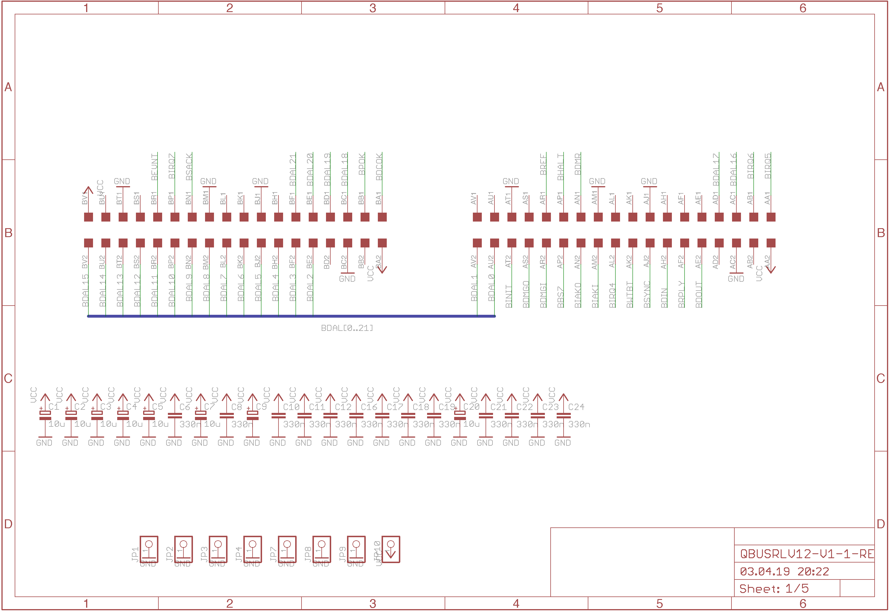
The first page just shows the Q-Bus connector the decoupling capacitors and some through hole points used as high current via’s.
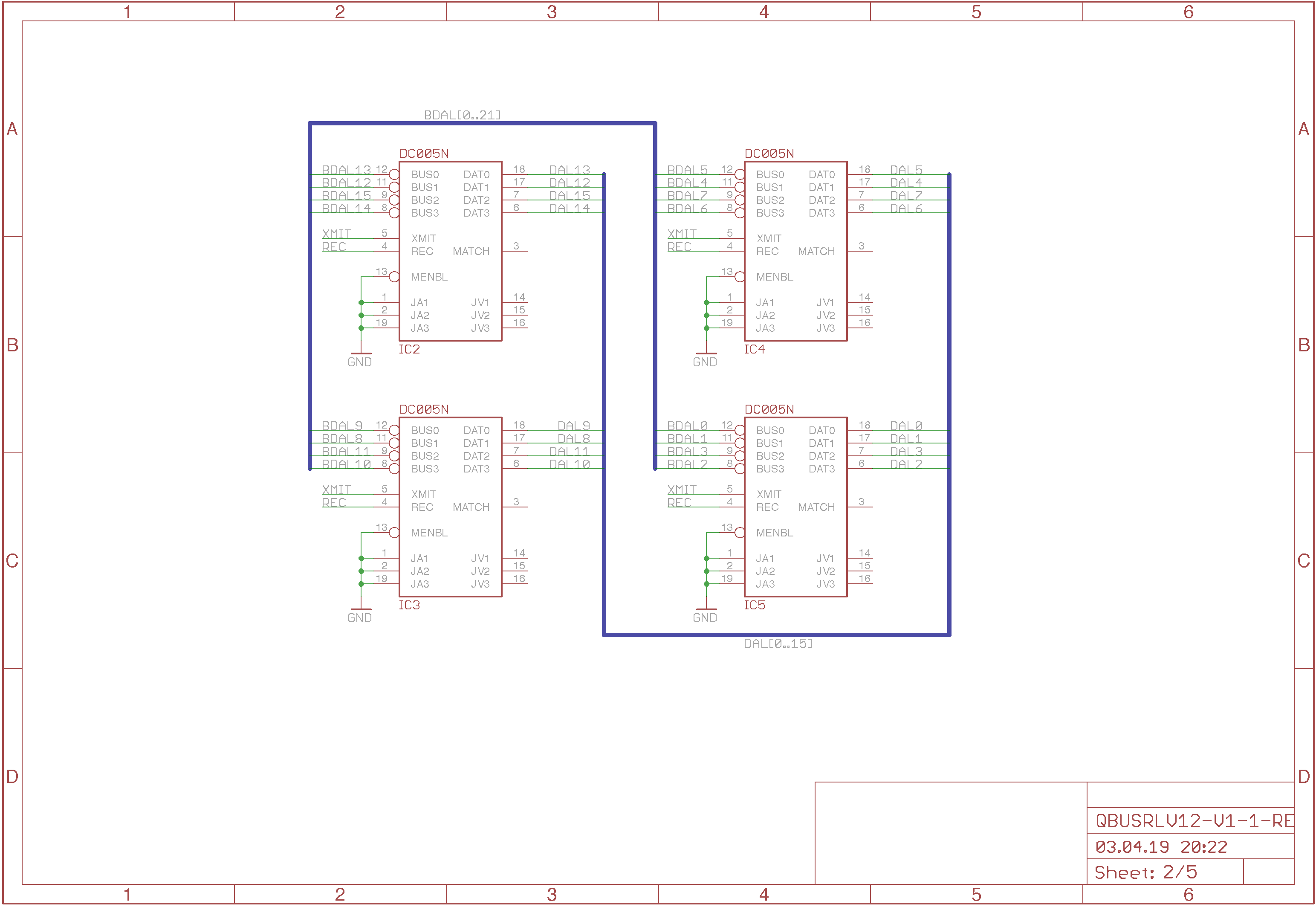
The second page shows the 16-bit address/data interface using the DC005. I only make
use of the Q-Bus interface, all the other features, like address matching and
interrupt vector generation are not used
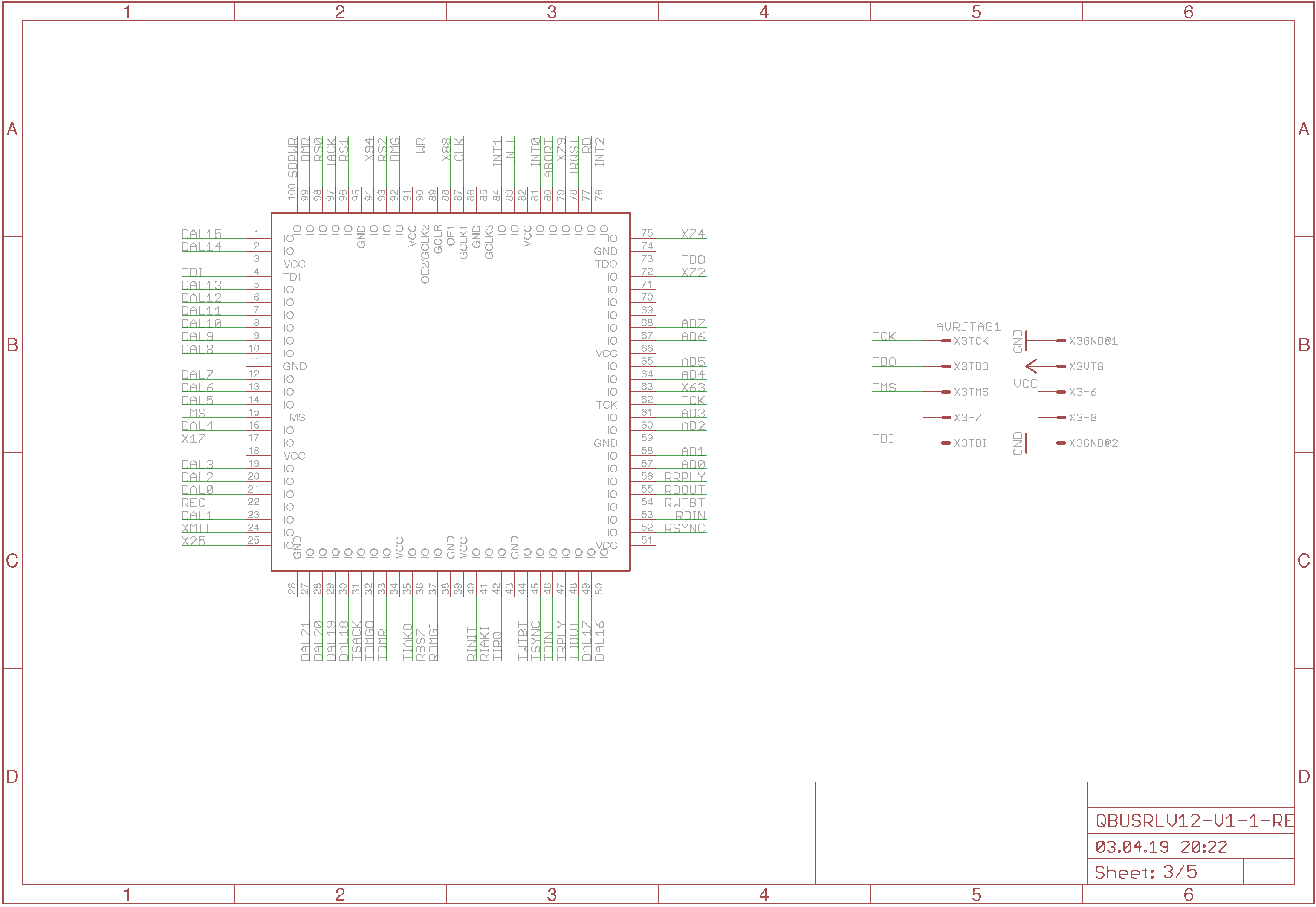
Just the signal names of the CPLD pins and the JTAG interface
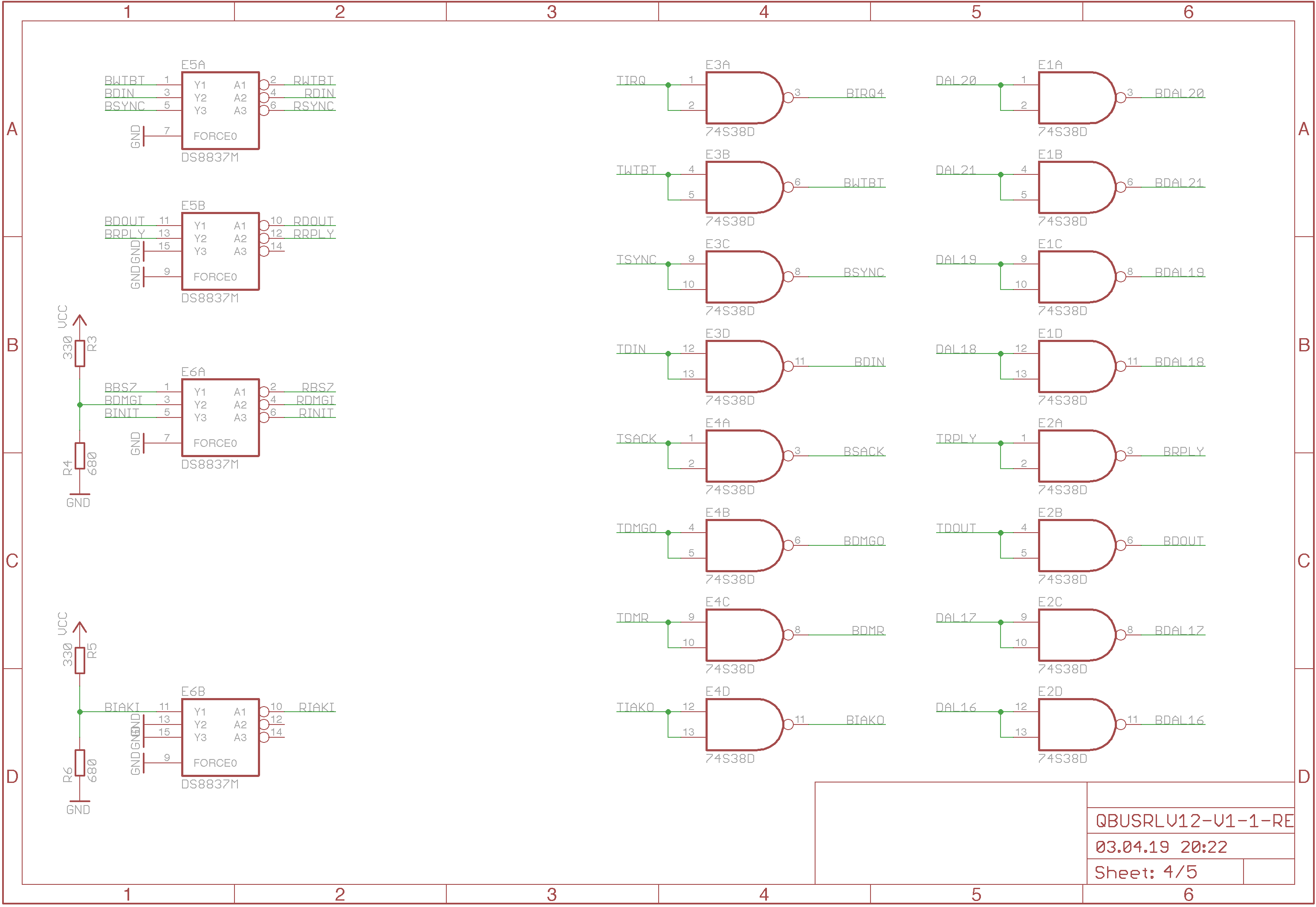
The remaining Q-Bus interface circuit with the DS8837 receivers and the 74S38
transmitters
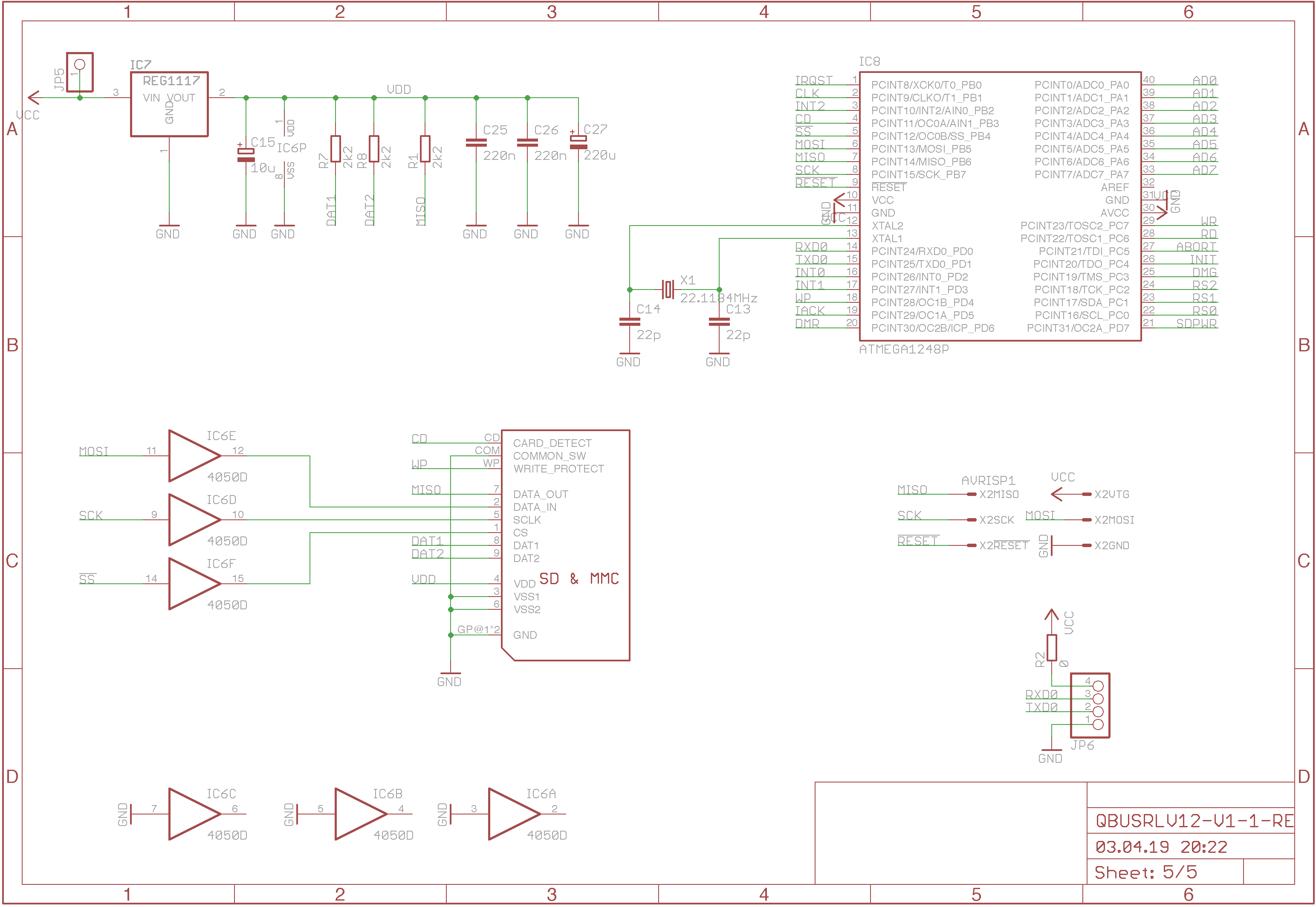
The microcontroller and the SD-Card interface. SD-Cards require 3.3V to operate
so I had to add level shifters. Note that it is very important to use the 74HC
and not the CD type for the buffers used.
PCB Layout
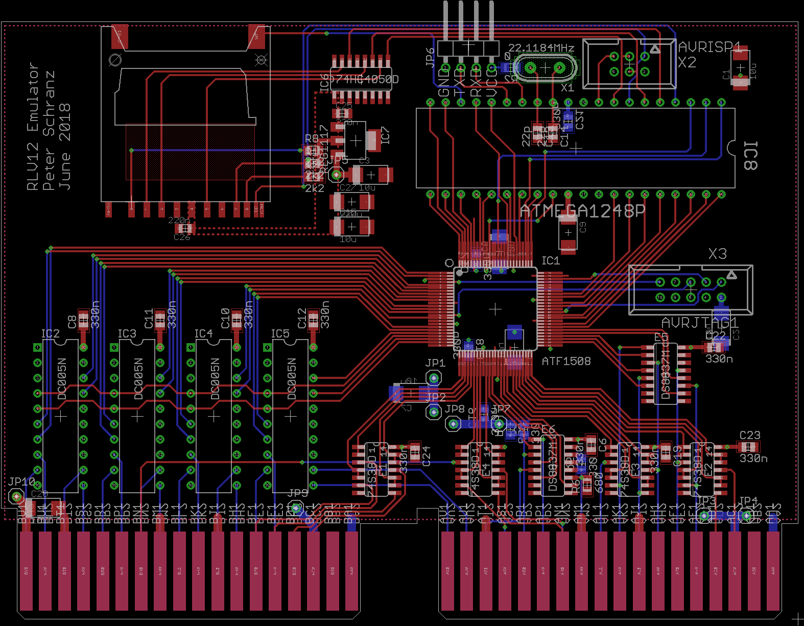
When I was doing the layout I was not considering the fact what will happen if it is inserted into a Q-Bus system. Consequently the ISP and JTAG programming connectors cannot be used and also to swap the SD-Card you need a long tweezer or you use a SD-Card extender cable. However, when using the extender cable you probably need to select a lower clock rate for the SPI interface. The current setting of half the MCU clock does not support long signal paths. This is a known issue with SPI. I have not measured the performance impact, but during development I often set the SPI clock to 1/4th of the MCU clock and when booting RSX-11Mplus I cannot really say it is slower.
Errata
Note that the labeling of the TTL Serial connector on the first 5 prototype PCBs is wrong it should say
GND TXD RXD VCC
The labels on these prototype boards are the reverse order. The picture shows the corrected version as well as the Eagle files in the download section.