PDP-11 Q-Bus Memory
This project had two goals. First I wanted a memory board for my Plessey system and second I started to look into alternatives to the Q-Bus transceivers which are no longer produced. The memory card starts with replacing the Q-Bus receivers I used in the RLV12 Emulator. The DS8837 are very difficult to find, especially the SMD versions. The reason I started with the receivers is very simple. For transmitters the 74S38 was always used by various vendors of Q-Bus interface cards and the 74S38 is still in production and available. So for simple transmitters there already is a feasible solution. The memory card still makes use of DC005 (aka Signetics C2324N) transmitters, but once the new receivers concept had been tested there would be a way to also replace these, although with some “overhead” in regards of number of ICs and signals required to interface to the rest of the logic, but with todays possibilities even for a hobbyist a much better option than expensive NOS ICs. However the DC005 are really versatile and fortunately they regularly pop-up in auctions for a reasonable price.
Update 2024
Unfortunately I never published the CPLD design file for 4Mbyte. Below you will find now both design files, one for a 2MByte card with only one RAM chip and another for a 4Mbyte card using both RAM chips.
Specifications
The board should support the full 4Mbyte address space of a 22-bit PDP-11 system. Normally PDP-11 memory used dynamic RAM. But today dynamic RAM for such a small memory are no longer available. Also I wanted this design to be still a pure 5 volts design. Therefore I decided to use 1M x 16 static RAM. They are available for 5 volts, not very expensive and are available in small quantities. The board can either be equipped with one or two SRAM, giving a total of 2Mbyte or 4Mbyte. The configuration is jumper less, i.e. you need to program the CPLD accordingly. The layout of the RAM was made with block mode DMA in mind. The connectivity to the bus for this function is in place. It’s just a matter of the CPLD logic design. And this is just a matter of time.
New Receivers
This board uses the 74HC4049 as bus receivers. The 74HC4049 is a hex inverter with over-voltage tolerant inputs. Inputs are over-voltage tolerant to 15 V. This enables the device to be used in HIGH-to-LOW level shifting applications.
Q-Bus receivers require an input threshold of 1.7V. The 74HC4049 are C-MOS devices with a threshold of approx. 50% of the power-supply voltage. So basically the idea was to operate the 74HC4049 at twice the threshold voltage. In my case I used a 3.3V LDO regulator. As a CMOS device the outputs will be rail to rail or in other words the high-level output voltage will be close to 3.3V and as such sufficiently high to drive standard TTL inputs.
The 74HC4094 is the HCMOS version of the legacy CD4049 CMOS. They have the same over-voltage tolerant inputs but require an operating voltage from 2V to 6V and are much faster at lower voltages. At 3.3V they are still as fast as standard DS8837 bus receivers. So this seemed to be the perfect hack to replace those unobtainable DS8837.
Currently Built Memory Cards
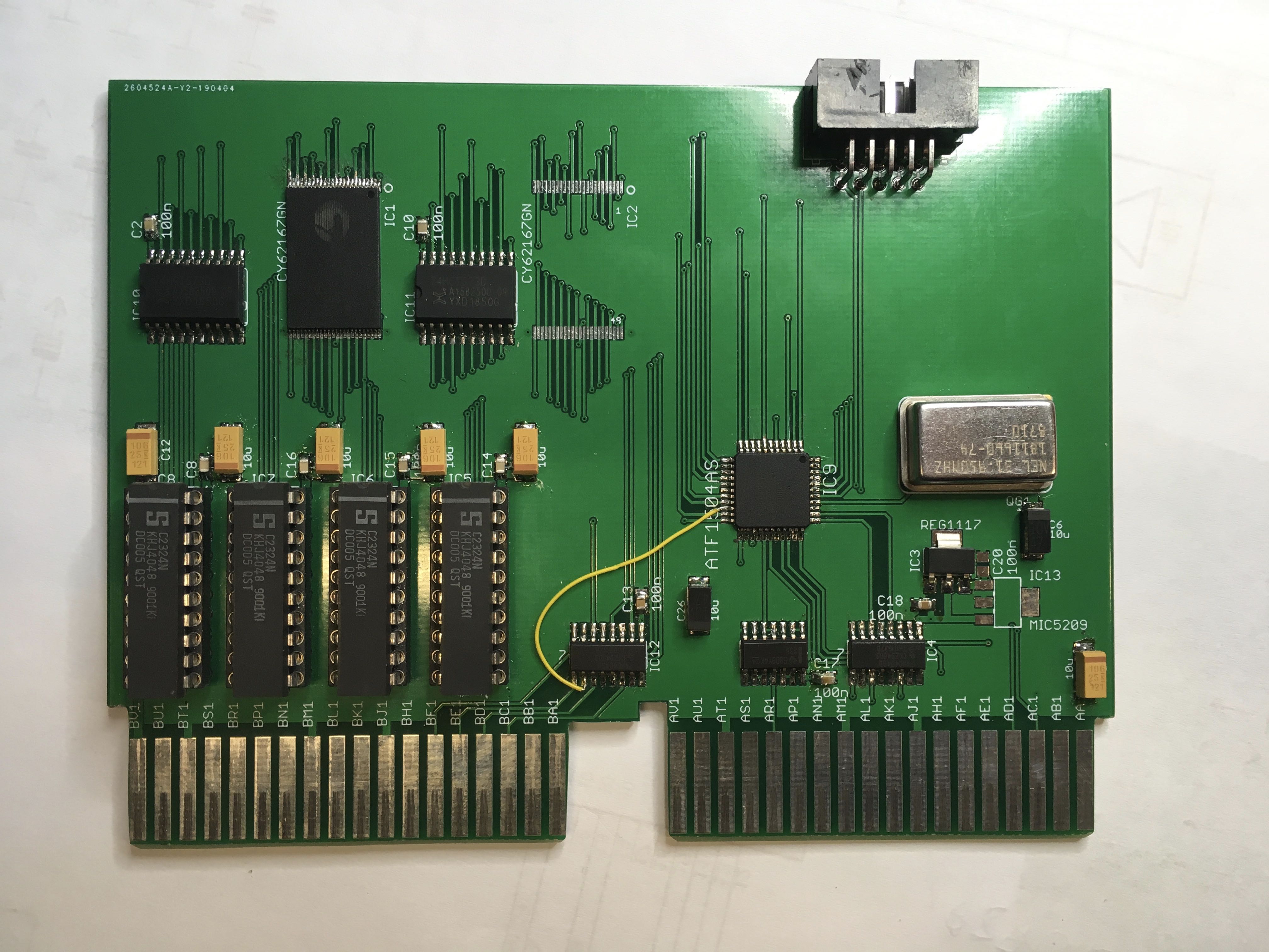
The following is a picture of the first board assembled. The yellow Kinar wire seems like an engineering change, but is in fact not required. It was just added to test finer granularity of size and start address. So instead of having only the options to support 2Mbyte or 4Mbyte I wanted to elaborate the options of having a 1Mbyte granularity.
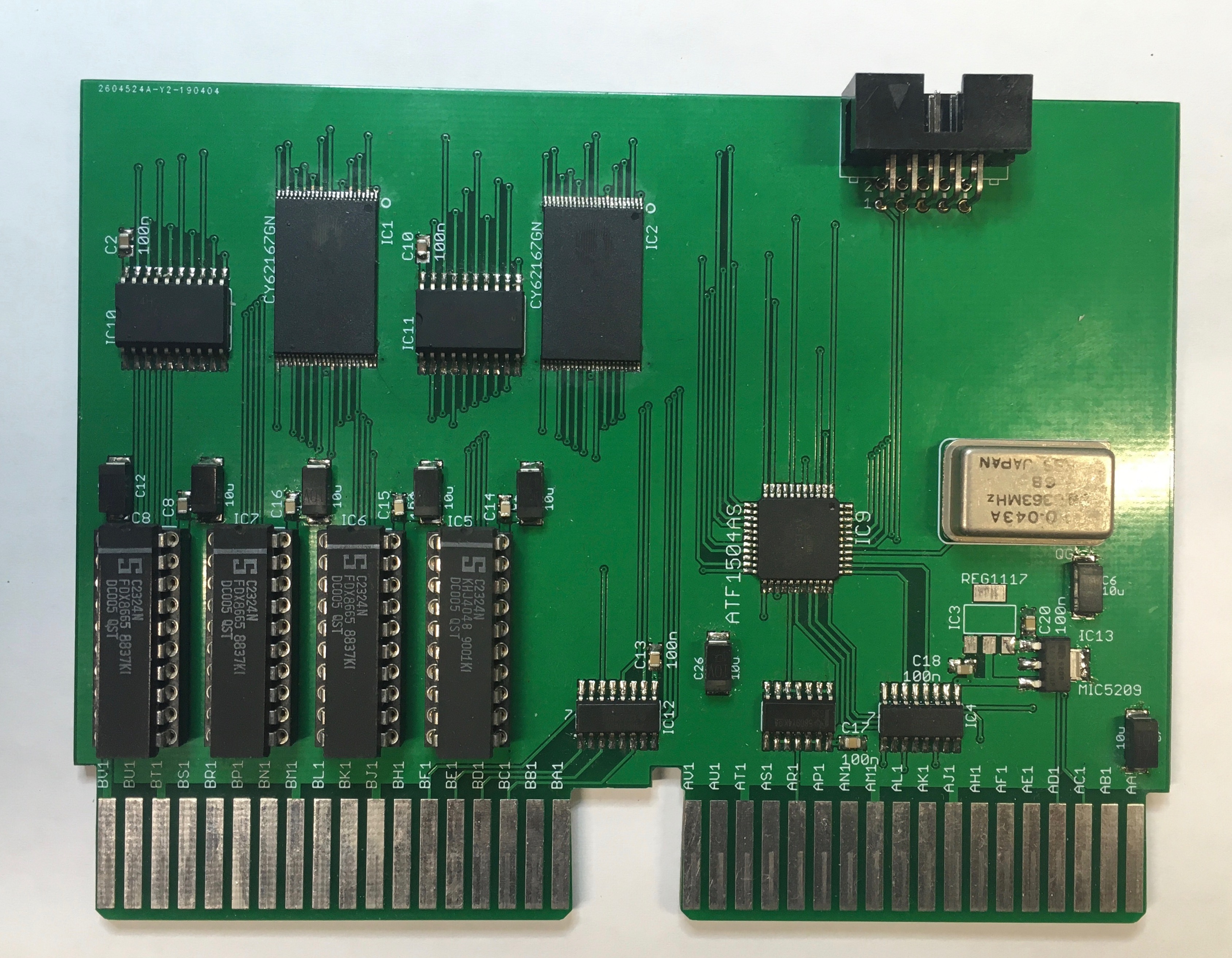
The following is a picutre of a fully populated memory card with 4Mbyte of SRAM.
Schematic
The board is quite simple. The SRAM used have two chip enable and one is currently tied to VCC via R1. This input would be very useful to support battery backup. A simple microprocessor supervisor chip like the MAX703 would be enough to add battery backup.
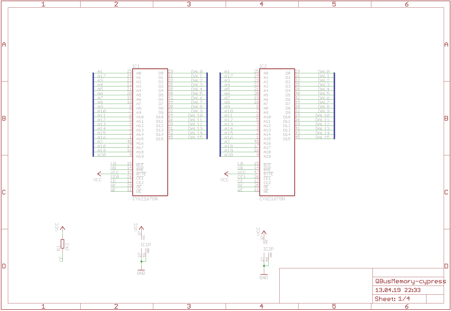
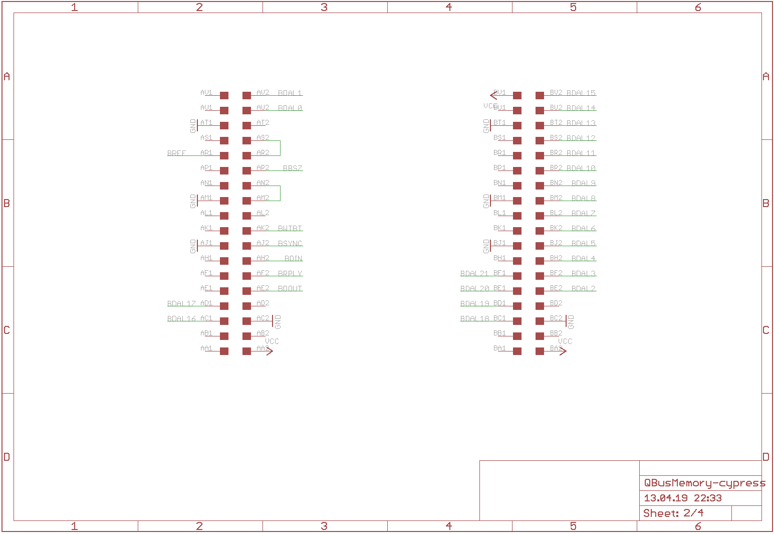
For a memory board we have to latch all 22 address bits. In my case I use two additional transparent latches (74HCT573) to latch address bits A5 to A20. The other address bits are latched internally by the CPLD. Address bit A0 is used for byte writes. Address bits A1 to A4 will then later be auto-incremented when I add DMA block transfer support. Address bit A21 is used to select either of the two SRAM chips.
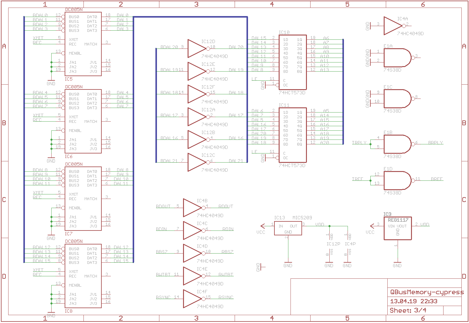
The CPLD requires a clock to create the necessary delays and overlapping of signals and bus enables to fulfill the Q-Bus timing requirements. The clock rate is not critical, any clock between 20MHz and 40MHz will do.
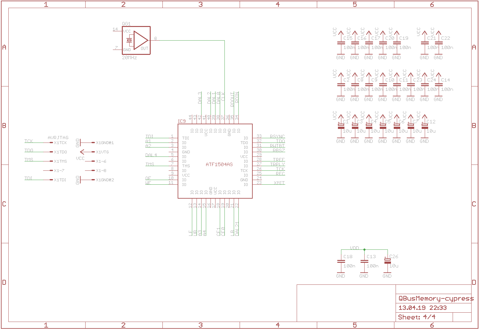
CPLD Design File
The current CPLD design only supports normal DATI and DATO/DATOB cycles. However the circuit has been made with block mode DMA in mind and all necessary signals connect to the CPLD and connect with the Q-Bus if required.
There are two variants, one is for 2Mbyte using only one RAM chip and the other is for 4Mbyte memory cards using two RAM chips.
Here is the 2Mbyte variant:
Name     QBUS Memory ;
PartNo   01 ;
Date     27.03.2019 ;
Revision 01 ;
Designer cbscpe ;
Company  PRIVAT ;
Assembly None ;
Location ATHOME ;
Device   f1504isptqfp44 ;

PROPERTY ATMEL {preassign KEEP};

PIN    38 =  DAL0;
PIN    39 =  DAL1;
PIN    40 =  DAL2;
PIN    42 =  DAL3;
PIN     5 =  DAL4;
PIN    22 =  DAL21;
PIN    20 =  DAL20;
PIN    37 =  CLK;

PIN     2 =  A1;
PIN     3 =  A2;
PIN    14 =  A3;
PIN    15 =  A4;

PIN    33 =  RSYNC;
PIN    30 =  RBS7;
PIN    31 =  RWTBT;
PIN    34 =  RDIN;
PIN    35 =  RDOUT;
PIN    27 =  TRPLY;
PIN    28 =  TREF;

PIN    19 = !CE0;
PIN    18 = !CE1;
PIN    10 = !OE;
PIN    11 = !WE;
PIN    21 = !LB;
PIN    13 = !UB;

PIN    23 =  XMIT;
PIN    25 =  REC;
PIN    12 =  LE;

PINNODE   =  A0;
PINNODE   =  A20;
PINNODE   =  A21;
PINNODE   =  BS7;
PINNODE   =  RDIN0, RDIN1, RDIN2;
PINNODE   =  RDOUT0, RDOUT1, RDOUT2;


[BS7, A21, A20, A4, A3, A2, A1, A0].le = !RSYNC;
[BS7, A21, A20, A4, A3, A2, A1, A0].l  =  [RBS7, DAL21, DAL20, DAL4, DAL3, DAL2, DAL1, DAL0];

[RDIN2..0].ck  =  CLK;
[RDOUT2..0].ck =  CLK;

RDIN0.d        =  RDIN;
RDIN1.d        =  RDIN0;
RDIN2.d        =  RDIN1;

RDOUT0.d       =  RDOUT;
RDOUT1.d       =  RDOUT0;
RDOUT2.d       =  RDOUT1;


XMIT           =  RSYNC  & !BS7  & !A21 & RDIN
               #  RSYNC  & !BS7  & !A21 & RDIN2;

REC            = !RDIN   & !RDIN2;

CE0            =  RSYNC  & !BS7  & !A21;

LB             =  RDIN2
               #  RDOUT  &  RWTBT & !A0
               #  RDOUT  & !RWTBT;

UB             =  RDIN2
               #  RDOUT  &  RWTBT &  A0
               #  RDOUT  & !RWTBT;

WE             =  RDOUT;
OE             =  RDIN2;

LE             = !RSYNC;

TRPLY          =  RSYNC  & !BS7  & !A21 &  RDIN0
               #  RSYNC  & !BS7  & !A21 &  RDOUT2;

TREF           = 'b'0;
And here is the 4Mbyte variant:
Name     QBUS Memory ;
PartNo   01 ;
Date     27.03.2019 ;
Revision 01 ;
Designer cbscpe ;
Company  PRIVAT ;
Assembly None ;
Location ATHOME ;
Device   f1504isptqfp44 ;

PROPERTY ATMEL {preassign KEEP};

PIN    38 =  DAL0;
PIN    39 =  DAL1;
PIN    40 =  DAL2;
PIN    42 =  DAL3;
PIN     5 =  DAL4;
PIN    22 =  DAL21;
PIN    20 =  DAL20;
PIN    37 =  CLK;

PIN     2 =  A1;
PIN     3 =  A2;
PIN    14 =  A3;
PIN    15 =  A4;

PIN    33 =  RSYNC;
PIN    30 =  RBS7;
PIN    31 =  RWTBT;
PIN    34 =  RDIN;
PIN    35 =  RDOUT;
PIN    27 =  TRPLY;
PIN    28 =  TREF;

PIN    19 = !CE0;
PIN    18 = !CE1;
PIN    10 = !OE;
PIN    11 = !WE;
PIN    21 = !LB;
PIN    13 = !UB;

PIN    23 =  XMIT;
PIN    25 =  REC;
PIN    12 =  LE;

PINNODE   =  A0;
PINNODE   =  A20;
PINNODE   =  A21;
PINNODE   =  BS7;
PINNODE   =  RDIN0, RDIN1, RDIN2;
PINNODE   =  RDOUT0, RDOUT1, RDOUT2;


[BS7, A21, A20, A4, A3, A2, A1, A0].le = !RSYNC;
[BS7, A21, A20, A4, A3, A2, A1, A0].l  =  [RBS7, DAL21, DAL20, DAL4, DAL3, DAL2, DAL1, DAL0];

[RDIN2..0].ck  =  CLK;
[RDOUT2..0].ck =  CLK;

RDIN0.d        =  RDIN;
RDIN1.d        =  RDIN0;
RDIN2.d        =  RDIN1;

RDOUT0.d       =  RDOUT;
RDOUT1.d       =  RDOUT0;
RDOUT2.d       =  RDOUT1;


XMIT           =  RSYNC  & !BS7  & RDIN
               #  RSYNC  & !BS7  & RDIN2;

REC            = !RDIN   & !RDIN2;

CE0            =  RSYNC  & !BS7  & !A21;

CE1            =  RSYNC  & !BS7  &  A21;


LB             =  RDIN2
               #  RDOUT  &  RWTBT & !A0
               #  RDOUT  & !RWTBT;

UB             =  RDIN2
               #  RDOUT  &  RWTBT &  A0
               #  RDOUT  & !RWTBT;

WE             =  RDOUT;
OE             =  RDIN2;

LE             = !RSYNC;

TRPLY          =  RSYNC  & !BS7  &  RDIN0
               #  RSYNC  & !BS7  &  RDOUT2;

TREF           = 'b'0;