Q-Bridge Description
PDP-11 Interface
A typical PDP-11 interface board or controller has one or more of the following building blocks
- A set of registers that are accessed via the so called IO page of a PDP-11. A PDP-11 does not have any special IO instructions it treats the registers in the IO page like any other addressable storage
- An interrupt logic that rises an interrupt and returns a vector during the interrupt acknowledge cycle
- A DMA interface which allows the controller to directly read and write from the PDP-11 main memory
- An interface to the peripheral, like RS-232, SCSI, SMD, MFM, QIC, Floppy Disk, Tape interface, etc.
- Local functions like ROM, RAM, Clock, etc.
Note this is an interface to the Q-Bus. If you want to interface in a generalized way to the UNIBUS you should have a look at Jörg Hoppe’s UNIBONE.
µcontroller Interface
Towards the microcontroller the CPLD looks like an interface device with internal registers, interrupt lines and control signals.
Peripheral Registers
The register interface of the Q-Bridge uses a 8-bit wide data bus, register select inputs to address the desired register and a read and a write signals.
The Atmega162 or Atmega1280 for example have an external memory interface that can be used to directly interact with a register interface of any peripheral. Simple lds and sts load and store SRAM instructions can be used to access individual registers of the Q-Bridge.
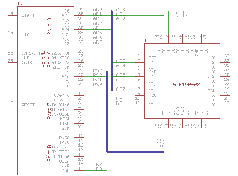
The following schematic illustrates the signals in use.
There are various ways to use the external memory interface. In this exmaple the external memory interface is set to use 12 address bits. The lower 8 address bits are multiplexed with the data and are not used, only the upper 4 bits of the 12-bit address are used to select the appropriate register.
A write pulse on WR latches the data to the addressed register and when
asserting RD the CPLD enables the outputs and presents the content of
the addressed register.
;
; Using the address bits A8..A11 of the external register interface creates the
; following addresses for the individual registers
;

.equ	REG0	= 0x8000
.equ	REG1	= 0x8100
.equ	REG2	= 0x8200
...
...
The advantage of the external memory interface is that access to the CPLD registers is using a single instruction, that is normal and interrupt routines may access the CPLD at the same time. The PDP-11/Hack multi-function board for example makes use of the external memory interface of the Atmega1280.
In case the microcontroller has no external memory interface the WRand RD
signals must be asserted and de-asserted by hand as well as the direction of
the data bus. This is the case for the Atmega1284P used in the RLV12
emulator.
The connection is still the same, you have an 8-bit data bus, register select signals, a RD and a WR control signal. But instead of using the lds and sts instructions you need to use sbi, cbi, out and in instructions to change the pins, data direction and transfer the data. And therefore the access must be protected from interrupts if interrupts can occur. The following shows the code used to program the DMA start address in the RVL12 emulator.
	ldi		temp, (1<<RS2) | (0<<RS1) | (0<<RS0)
	cli								;;;
	out		PORTC, temp				;;;
	out		DDRA, ff				;;; PORTA is output
	lds		temp, BARL				;;; A1..A7
	bld		temp, 0					;;; DMA Direction
	out		PORTA, temp				;;;
	sbi		b_WR
	sbi		PORTC, RS0				;;; RS4->RS5
	lds		temp, BARH				;;; A8..A15
	out		PORTA, temp
	sbi		PORTC, RS1				;;; RS5->RS7
	lds		temp, BAEL				;;; A16..A21
	out		PORTA, temp
	cbi		b_WR
	sei
Note that very often the registers are not read-write registers. That is when reading register 0 it will not return the value written to register 0 previously. This is mostly a limitation of the CPLD resources as you should limit the number of registers you can read to five.
Q-Bridge Register Model
The basic Q-Bridge implements the following registers
| Register | Direction | Description |
|---|---|---|
| Device Address | Read | On every BSYNC the CPLD latches the lower address registers and makes them available to the MCU. Normally I latch address bits BDAL0..6 but the register provides BDAL1..6 and the two MSB are used to indicated which bytes in a DATO/DATOB is cycle needs to be updated |
| Q-Bus In | Read | This are two bytes that read the current value of BDAL0..15. These registers are used during a DATO cycle to fetch the data. In some designs these registers are also used to read the DMA data from the BUS during the data transfer portion of a DMA read cycle |
| Q-Bus Data | Write | This are two bytes that are loaded by the MCU to provide the data during a DATI cycle. In some designs these registers are also used during the data transfer portion of a DMA write cycle |
| DMA Address | Write | These are three registers that are written by the MCU to set the initial address of a DMA cycle. The Q-Bridge only implements only 16-bit DMA transfers. The LSB is used to program the direction of the DMA. |
| DMA Read Data | Read | The last design of the Q-Bridge which adds a second CPLD implements a DMA read data register. The advantage is that the MCU now only needs to set the DMA address and then trigger a DMA cycle. The DMA cycle is completely handled within the CPLD and when the DMA has finished the CPLD signals the MCU via a control signal that the DMA data is ready to be read via these two byte registers |
| DMA Write Data | Write | The last design of the Q-Bridge which adds a second CPLD implements a DMA write data register. These two bytes must be loaded with the DMA data to be written before a DMA cycle is triggered. The CPLD then will automatically execute the DMA cycle and inform the MCU when the cycle has finised |
External Interrupts
In addition to the register interface there are interrupt signals which allows the Q-Bridge to rise an attention to the microcontroller. These pins are typically connected to the external interrupt pins named INT0, INT1 and INT2 of the AVR processors. Generally I use INT0 to signal a DATO/DATOB and INT1 to signal a DATI cycle to the PDP-11 interface.
In case of the multi-function board INT2 is used to signal a DATI to the BootROM and in case of the RLV12 emulator INT2 is used to signal a IAKI cycle.
In some cases I use the Pin Change interrupt which is connected to BINIT to inform the MCU about the rising and falling edge of the BINIT signal. This is mostly used to reset the status of the emulated device.
Control and Handshaking Signals
There is also a set of dedicated control and handshaking signals. This is mainly to make use of the very efficient sbic and sbis instructions (skip on IO bit cleared or skip on IO bit set) and the sbi and cbi, set IO bit and clear IO bit that are much faster than reading a status register and test individual bits or manipulate individual bits in a control register. Another advantage is that individual signals use less resources in the CPLD than a register.
| Signal name | Description |
|---|---|
| IACK | A short pulse clears any of the pending interrupts (INT0, 1, 2) |
| IRQST | Request an interrupt to the PDP-11 |
| ABORT | Abort a DMA bus cycle, e.g. when we detect a bus timeout |
| INIT | Forwarded Q-Bus BINIT initialisation request |
| DMR | Start a DMA request |
| DMG | DMA granted/progress |
| RD | Read data from the selected register of the CPLD |
| WR | Write data to the selected register of the CPLD |
Q-Bus Interface
Device Registers
First let’s start what happens if the PDP-11 accesses one of the device registers of the interface adapter.
When the PDP-11 CPU reads or writes to the registers of a controller on the Q-Bus it basically does the following
- Places the addresses onto the address/data lines and in case of a write request asserts BWTBT and asserts BSYNC
- In case of a read request, called DATI in Q-Bus jargon, it asserts BDIN and waits until the addressed device places that data onto the bus and asserts BRPLY
- In case of a write request, called DATO/DATOB, it places the data onto the bus and asserts BDOUT, it then waits for the device to retrieve the data and assert BRPLY
- When the BRPLY is asserted it will de-assert either BDIN or BDOUT, remove the data from the bus and de-assert BSYNC
Together with the addresses the PDP-11 also asserts BBS7 when accessing the
device registers in the IO-Page and in case of a
DATO/DATOB also BWTBT. The CPLD will monitor BBS7 and the lower 13 bits of
the address and match them with the range of device register addresses.
Depending on the status of BWTBT it will trigger INT0 for writes and
INT1for read access the moment BSYNCis asserted. At the same time it will
latch the necessary address bits in an internal register so the microcontroller
can retrieve the register address. Here are the corresponding excerpts of the
Q-Bridge CPLD used in the RLV12 Emulator.
PINNODE       =  [C5..0];        /* CSR Address                                  */

FIELD  ADDR   = [C5..0];         /* Latched address used for register address    */
FIELD  IOADDR = [DAL15..0];      /* Address Bus                                  */

ADDR.d        =  [DAL5..0].io;
ADDR.ck       =  RSYNC;

CSRADDR       =  IOADDR.io:['o'174400..174417];
CS1ADDR       =  IOADDR.io:['o'174400..174401];

CSR.ck        =  RSYNC;
CSR.d         =               RBS7 &  CSRADDR;

CS1.ck        =  RSYNC;
CS1.d         =               RBS7 &  CS1ADDR;

INT1.d        = !(!RWTBT &  RBS7 &  CSRADDR & !CS1ADDR);
INT1.ck       =  RSYNC;
INT1.ap       =  IACK;

INT0.d        =  !(RWTBT &  RBS7 &  CSRADDR);
INT0.ck       =  RSYNC;
INT0.ap       =  IACK;

UB            = !RWTBT
              #  RWTBT  &  C0;
LB            = !RWTBT
              #  RWTBT  & !C0;

[AD7..0]      =  RS:['d'0] &  [DAL7..0].io
              #  RS:['d'1] &  [DAL15..8].io
              #  RS:['d'4] &  [UB, LB, C0, C5, C4, C3, C2, C1];

[AD7..0].oe   =  RD;
In the example above you will notice that no interrupt will be triggered if the base CSR is read. This special setup is made so the PDP-11 can poll the base CSR for command completion without interrupting the microcontroller. We will come to this detail later.
In the other cases this triggers an interrupt and either the INT0 or INT1 interrupt service routine will be executed by the Microcontroller.
;--------------------------------------------------------------------------
;
;	Interrupt Routines DATO/DATOB
;
;	INT0 covers DATO/DATOB cycles. Note that RLV12 registers are only word
;	addressable so we do not need to cover the DATOB cycle. The RLV12
;	just accepts any data written to the registers as long as the bits
;	are read-write. The PDP-11 initiates a command by clearing CRDY. When
;	this bit is clearedd the controller is busy and does no longer accept
;	access to the registers.
;
INT0_isr:
	sbrs	cs1_l, CSR_CRDY
	reti				;;; do nothing when controller busy i.e. CRDY==0
	in	isreg, SREG		;;; Save processor status
;
;	Register 4 holds the CSR address and the byte access bits.
;	LB is set when the lower/even byte needs to be written
;	UB is set when the upper/odd byte needs to be written
;	In case of a 16-bit word write both bits are set
;	The bits are arranged in a way that the lower bits can
;	be used as an CSR word index. BA0 is there for convenience only
;	but typically not needed.
;
;	+---+---+---+---+---+---+---+---+
;	| UB| LB|BA0|BA5|BA4|BA3|BA2|BA1|
;	+---+---+---+---+---+---+---+---+
;
.equ	UB	= 7			; Write Upper Byte
.equ	LB	= 6			; Write Lower Byte

	out	DDRA, zero		;;; Port A will be used as input
	ldi	itemp, (1<<RD) | (1<<RS2) | (0<<RS1) | (0<<RS0)
	out	PORTC, itemp		;;; Reg register 4 = CSR Address and status
	push	zl
	push	zh			;;; We need the Z pointer
	in	zl, PINA		;;; Get the CSR address and status bits
	out	GPIOR0, zl		;;; Save in "fast" location
	andi	zl, 0x07		;;; Only keep latched address A1, A2, A3
	clr	zh						;;;
	subi	zl, low(-INT0_table)
	sbci	zh, high(-INT0_table)	;;; and convert to index into jump table
	ldi	itemp, (1<<RD) | (0<<RS2) | (0<<RS1) | (1<<RS0)
	out	PORTC, itemp		;;; prepare the port to read BDAL15..8
	ijmp				;;;

INT0_table:
	rjmp	csrout
	rjmp	barout
	rjmp	darout
	rjmp	mprout
	rjmp	baeout
	rjmp	bae2out
	rjmp	bae4out
	rjmp	bae6out
The interrupt routine will first read the CSR address register (4). In this case the microcontroller is an Atmega1284P and as already mentioned the interface to the CPLD uses GPIO pins of the ports. Therefore it has to first setup the data port direction register, the register select address and assert the read signal. Then it reads the CSR address register via Port A. Note that the synchronisation circuit of the Atmega requires you to wait in order to read the input pins. This time is used to save the Z pointer registers. The CSR address is used as an offset into a jump table where the appropriate register is handled. But first we setup the register interface to read register 1 which is the high byte of the Q-Bus data written by the PDP-11.
;
;	BAE	17774410
;
baeout:
	in	itemp, PINA
	cbi	PORTC, RS0
	sts	BAEH, itemp
	in	itemp, PINA
	sts	BAEL, itemp
	bst	itemp, BAE_BA16
	bld	cs1_l, CSR_BA16
	bst	itemp, BAE_BA17
	bld	cs1_l, CSR_BA17

	.if	loggreg==1		;;;
	lds	loglow, BAEL
	.endif				;;;

	UPDCS1
	INT0_exit
In the example I show the processing when writing the bus address extension
register. First we need to read the word written by the PDP-11 from the Q-Bus.
This is done by reading the high byte from the bus, change the register address
from 1 to 0 and then read the low byte from the bus. We store the values in
local SRAM locations BAEH and BAEL and we also copy the bits for address bits
16 and 17 to the local copy of the base CSR register. In the case of the RLV12
emulator we do not need to check for byte access as all the RLV12 registers
can be accessed only as words. UPDCS1 and INT0_exit are
two macros which generate the following code.
.macro	UPDCS1
	out	DDRA, ff
	out	PORTA, cs1_l
	ldi	itemp, (0<<RS2) | (1<<RS1) | (0<<RS0)
	out	PORTC, itemp
	WRTCPLD
	ldi	itemp, (0<<RS2) | (1<<RS1) | (1<<RS0)
	out	PORTA, cs1_h
	out	PORTC, itemp
	WRTCPLD
.endmacro				; 11 cycles
UPDCS1 just updates the base CSR register in the CPLD which we need to keep
in sync with every update we make to your local copy. Remember the base CSR
is read directly via the CPLD and does not interrupt the microcontroller and
in case of updating the BAE (bus address extension) register we need to update
the base CSR as it has a copy of bus address bits 16 and 17.
The second macro does some postprocessing, restores the registers and the status and ultimately acknowledges the interrupt in the CPLD and returns from the interrupt.
.macro	INT0_exit			;;;
	pop	zh			;;; Restore Z pointer
	pop	zl
	out	SREG, isreg		;;; Restore processor status
	sbi	b_IACK			;;; Signal the CPLD to assert RPLY
	cbi	b_IACK
	reti				;;; Exit interrupt
.endmacro
When the microcontroller acknowledges the interrupt the CPLD will assert BRPLY
and the PDP-11 bus cycle will be finished.
TRPLY         =  CSR &  RSYNC &  INT1 &  RDIN	/* Assert RPLY when MCU is done      */
              #  CSR &  RSYNC &  INT0 &  RDOUT;	/* Assert RPLY when MCU is done      */
The interrupt service routine must finish before a bus timeout occurs. That is the total processing must finish well within the limits of the 8 to 10µs. This however holds only if the interrupt service routine is immediately started when the interrupt occurs. Therefore it is very important that the microcontroller never disables interrupts for an extended period. Interrupts however have to be disabled if the main program requires access to resources shared with the interrupt service, e.g. the CPLD registers, or if another interrupt service routine is executed.
This has an impact on the design of the rest of the program. First disabling interrupts in the main program must be limited to very small program sequences and other interrupt service routines must only do minimal processing.
On the other hand 8µs for the Atmeag1248P running at 22.1184MHz as it is in the case of the RLV12 emulator is equivalent to about 170 CPU cycles. And you can do a lot in 170 CPU cycles on Atmeag1248P when programming in assembler. With the current design, including extended logging, DATI and DATO cycles take less than 4µsec.
Note how we encode the byte access into the upper two bits of the CSR address in case of a DATO/DATOB cycle. For DATO cycles both bits are set, for DATOB cycle only the bit corresponding to the byte written is set. A set bit means update the corresponding byte and a clear bit skip processing of the corresponding byte. So in case you need to support byte addressable CSR Registers you would use a code like shown here
	sbis	GPIOR0, UB
	rjmp	noupperbyte
	...
	...			; Update upper byte
noupperbyte:
	sbis	GPIOER0, LB
	rjmp	nolowerbyte
	...
	...			; Update lower byte
nolowerbyte:
CPLD Registers
The CPLD register interface for the microcontroller for the device register interface is very simple. The microcontroller can effectively only read 3 registers, the CSR address register and byte access codes, the lower and the upper 8-bit of the current 16-bit Q-Bus data.
UB            = !RWTBT
              #  RWTBT  &  C0;
LB            = !RWTBT
              #  RWTBT  & !C0;

[AD7..0]      =  RS:['d'0] &  [DAL7..0].io
              #  RS:['d'1] &  [DAL15..8].io
              #  RS:['d'4] &  [UB, LB, C0, C5, C4, C3, C2, C1];

[AD7..0].oe   =  RD;
On the other side the microcontroller can write to two 16-bit registers. The first is the data register which is used for DATI cycles. This is the value that is placed on the Q-Bus during PDP-11 reads. The second is the copy of the base CSR register that is held in the microcontroller and the CPLD in order for the PDP-11 to read the base CSR without interrupting the microcontroller
/*
	Q-Bus Data Register

 */
[D7..0].d     =  [AD7..0].io;
[D15..8].d    =  [AD7..0].io;
[D15..0].ck   =  WR;
[D7..0].ce    =  RS:['d'0];
[D15..8].ce   =  RS:['d'1];
/*
	Control and Status Register
 */
[DD7..0].d    =  [AD7..0].io;
[DD15..8].d   =  [AD7..0].io;
[DD15..0].ck  =  WR;
[DD7..0].ce   =  RS:['d'2];
[DD15..8].ce  =  RS:['d'3];
For DATI cycles the CPLD must select between the two registers control the output enable of the CPLD and the direction control signals of the DC005 used in the Q-Bus version of the RLV12 emulator
[DAL15..0]    = !RIAKI & !DMA3  &  CS1   &  [DD15..0]
              # !RIAKI & !DMA3  & !CS1   &  [D15..0]
              # !RIAKI &  DMA3  & !DMA2  &  [A15..1, 'b'0]
              # !RIAKI &  DMA3  &  DMA2  &  [D15..0]
              #  RIAKI                   &  'o'160;

XMIT          = !RIAKI          & !DMA3  &  CSR   &  RDIN  &  RSYNC
              #  RIAKI          & !DMA3  &  DACK  &  RDIN
              # !RIAKI & !DMA4  &  DMA3                    /* 0x08..0x0F DMA Write */
              # !RIAKI &  DMA4  &  DMA3  & !DMA2;          /* 0x18..0x1B DMA Read  */


RECI          =                   !DMA3           & !RDIN  /* During Non DMA       */
              #           DMA4  &  DMA3  &  DMA2;          /* Data phase DMA read  */

REC           =  RECI;

[DAL15..0].oe =  XMIT;
Note that this already shows additional terms of the equations used for
interrupt acknowledge and DAM. For the moment only consider the terms
with RIAKI and DMA3 equal 0.
Interrupt Logic
A real PDP-11 device also needs to support interrupts and provide an
interrupt vector during the interrupt acknowledge cycle. The interface
uses another external microcontroller interrupt INT2. First the
microcontroller sets the interrupt signal by asserting the special
control signal IRQST.
Whenver BDIN is asserted the status of this signal is latched into the
DACK register. In case the BDIN is asserted as part of the interrupt
acknowledge cycle it makes sure that the status does not change during
the acknowledge phase that is during the time BIAKI is asserted. When
BIAKI is asserted and we have requested the interrupt the CPLD asserts
INT2 and hands over the interrupt acknowledge to the microcontroller.
The microcontroller can do various things, e.g. it could update the base
CSR register as it is the case for existing PDP-11 devices. In all cases
the microcontroller must first release the interrupt, that is it must
de-assert IRQST and then it must clear INT2 which then finishes the
interrupt acknowledge cycle of the PDP-11. The above output logic of the
data bus makes sure that the correct vector is placed on the bus before
BRPLY is asserted.
DACK.d        =  IRQST;
DACK.ck       = !DMA3     &  RDIN;
DACK.ar       =  RINIT;

TIAKO         =  RIAKI    & !DACK;
TIRQ          =  IRQST;

INT2.d        = !DACK;
INT2.ck       =  RIAKI;
INT2.ap       =  IACK;

APPEND
TRPLY         =  RIAKI & !IRQST &  INT2 & RDIN;
The following shows the interrupt service routine for INT2 interrupts that are triggered by IAKI cycles
INT2_isr:
	cbi		b_IRQST				; De-assert IRQ
	in		isreg, SREG

	.if debug == 1
	lds		itemp, INT2_count	; Update interrupt counter
	inc		itemp
	sts		INT2_count, itemp
	.endif

	out		SREG, isreg
	sbi		b_IACK			; Acknowledge CPLD interrupt
	cbi		b_IACK
	reti
This shows the code used in the RLV12 emulator. When the emulator needs to raise an interrupt it simly sets IRQST. This will assert BIRQ4 on the Q-Bus. When the PDP-11 acknowledges the interrupt for this device INT2 triggers the MCU ISR. In our case we don’t do a lot of processing, but other PDP-11 controllers eventually change bits in device registers during the interrupt acknowledge cycle.
DMA
Last but not least the CPLD also allows the microcontroller to perform a DMA. For this the CPLD has another 3 registers the microcontroller can write. The DMA start address.
DMA is always word aligned. We use the LSB to define the direction. You will notice that writing the DMA address does not make use of the .ck and .ce equations typically used to write registers. The reason is that we need the .ck to autoincrement the DMA address. In other words, when the microcontroller wants to perform a DMA for a block of data, which is normally the case for block IO devices, it only needs to set the start address. And of course some logic is required to place the upper address bits onto the address bus.
/*
	DMA Address
 */
DMARW.ar      =  WR  &  RS:['d'4] & !AD0.io;
DMARW.ap      =  WR  &  RS:['d'4] &  AD0.io;
DMARW.ck      = 'b'0;
DMARW.d       = 'b'0;

[A7..1].ar    =  WR  &  RS:['d'4] & ![AD7..1].io;
[A7..1].ap    =  WR  &  RS:['d'4] &  [AD7..1].io;

[A15..8].ar   =  WR  &  RS:['d'5] & ![AD7..0].io;
[A15..8].ap   =  WR  &  RS:['d'5] &  [AD7..0].io;

[A21..16].ar  =  WR  &  RS:['d'7] & ![AD5..0].io;
[A21..16].ap  =  WR  &  RS:['d'7] &  [AD5..0].io;

/*
	Synchronous counter for DMA address which is updated after every DMA cycle. The address
	is incremented whenever a DMA cycle has finished.
 */
[A21..1].ck   = !DMA3;

A1.t          = 'b'1;
A2.t          = A1;
A3.t          = A1 & A2;
A4.t          = A1 & A2 & A3;
A5.t          = A1 & A2 & A3 & A4;
A6.t          = A1 & A2 & A3 & A4 & A5;
A7.t          = A1 & A2 & A3 & A4 & A5 & A6;
A8.t          = A1 & A2 & A3 & A4 & A5 & A6 & A7;
A9.t          = A1 & A2 & A3 & A4 & A5 & A6 & A7 & A8;
A10.t         = A1 & A2 & A3 & A4 & A5 & A6 & A7 & A8 & A9;
A11.t         = A1 & A2 & A3 & A4 & A5 & A6 & A7 & A8 & A9 & A10;
A12.t         = A1 & A2 & A3 & A4 & A5 & A6 & A7 & A8 & A9 & A10 & A11;
A13.t         = A1 & A2 & A3 & A4 & A5 & A6 & A7 & A8 & A9 & A10 & A11 & A12;
A14.t         = A1 & A2 & A3 & A4 & A5 & A6 & A7 & A8 & A9 & A10 & A11 & A12 & A13;
A15.t         = A1 & A2 & A3 & A4 & A5 & A6 & A7 & A8 & A9 & A10 & A11 & A12 & A13 & A14;
A16.t         = A1 & A2 & A3 & A4 & A5 & A6 & A7 & A8 & A9 & A10 & A11 & A12 & A13 & A14 & A15;
A17.t         = A1 & A2 & A3 & A4 & A5 & A6 & A7 & A8 & A9 & A10 & A11 & A12 & A13 & A14 & A15 & A16;
A18.t         = A1 & A2 & A3 & A4 & A5 & A6 & A7 & A8 & A9 & A10 & A11 & A12 & A13 & A14 & A15 & A16 & A17;
A19.t         = A1 & A2 & A3 & A4 & A5 & A6 & A7 & A8 & A9 & A10 & A11 & A12 & A13 & A14 & A15 & A16 & A17 & A18;
A20.t         = A1 & A2 & A3 & A4 & A5 & A6 & A7 & A8 & A9 & A10 & A11 & A12 & A13 & A14 & A15 & A16 & A17 & A18 & A19;
A21.t         = A1 & A2 & A3 & A4 & A5 & A6 & A7 & A8 & A9 & A10 & A11 & A12 & A13 & A14 & A15 & A16 & A17 & A18 & A19 & A20;


[DAL21..16]  =  [A21..16]       &  DMA3;
Fact is a ripple counter would be sufficient but I just wanted to explore the capapbilities of the CPLD.
Once the DMA address has been set the microcontroller must initiate a word transfer.
There are two control signals DMR and DMGto control the DMA and a state machine
that performs the DMA cycle.
TDMR.d        = 'b'1;
TDMR.ck       =  DMR;
TDMR.ar       =  DMA3 # RINIT # ABORT;

TSYNC.ck      =  CLK;
TDOUT.ck      =  CLK;
TDIN.ck       =  CLK;
/*
	Synchronous Signals
 */
DMGI.ck       =  CLK;
DMA.ck        =  CLK;
RPLY.ck       =  CLK;
DMG.ck        =  CLK;

DMA.ar        =  RINIT # ABORT;
 /*
 	Latched BDMGI and BRPLY as we need a stable DMGI and RPLY for the state machine
  */
DMGI.d        =  RDMGI;
RPLY.d        =  RRPLY;

sequence DMA {

   PRESENT 'h'00 IF !DMGI                    NEXT 'h'00;
                 IF  DMGI                    NEXT 'h'01;

   PRESENT 'h'01 IF !DMR                     NEXT 'h'02;
                 IF  DMR                     NEXT 'h'03;

   PRESENT 'h'02 IF !DMGI                    NEXT 'h'00;
                 IF  DMGI OUT TDMGO;         NEXT 'h'02;

   PRESENT 'h'03 IF !DMARW                   NEXT 'h'08;
                 IF  DMARW                   NEXT 'h'18;
/*
     Write
*/
   PRESENT 'h'08                             NEXT 'h'09           OUT DMG;

   PRESENT 'h'09                             NEXT 'h'0A           OUT DMG;

   PRESENT 'h'0A                             NEXT 'h'0B OUT TSYNC OUT DMG;

   PRESENT 'h'0B                             NEXT 'h'0C OUT TSYNC OUT DMG;

   PRESENT 'h'0C IF  DMR                     NEXT 'h'0C OUT TSYNC OUT DMG;
                 IF !DMR                     NEXT 'h'0D OUT TSYNC OUT DMG OUT TDOUT;

   PRESENT 'h'0D IF !RPLY                    NEXT 'h'0D OUT TSYNC OUT DMG OUT TDOUT;
                 IF  RPLY                    NEXT 'h'0E OUT TSYNC OUT DMG OUT TDOUT;

   PRESENT 'h'0E IF  RPLY                    NEXT 'h'0E OUT TSYNC OUT DMG;
                 IF !RPLY                    NEXT 'h'0F           OUT DMG;

   PRESENT 'h'0F                             NEXT 'h'00;
/*
     Read
*/
   PRESENT 'h'18                             NEXT 'h'19;

   PRESENT 'h'19                             NEXT 'h'1A;

   PRESENT 'h'1A                             NEXT 'h'1B OUT TSYNC;

   PRESENT 'h'1B                             NEXT 'h'1C OUT TSYNC;

   PRESENT 'h'1C IF !RPLY                    NEXT 'h'1C OUT TSYNC         OUT TDIN;
                 IF  RPLY                    NEXT 'h'1D OUT TSYNC OUT DMG OUT TDIN;

   PRESENT 'h'1D IF  DMR                     NEXT 'h'1D OUT TSYNC OUT DMG OUT TDIN;
                 IF !DMR                     NEXT 'h'1E OUT TSYNC OUT DMG;

   PRESENT 'h'1E IF  RPLY                    NEXT 'h'1E OUT TSYNC OUT DMG;
                 IF !RPLY                    NEXT 'h'1F           OUT DMG;

   PRESENT 'h'1F                             NEXT 'h'00;
}

TSACK         =          DMA3;
TWTBT         = !DMA4 &  DMA3 & !DMA2 & !DMA1;
DMA is initiated by the microcontroller asserting DMR. This asserts
BDMG and eventually we will receive a BDMGI. At that stage the state
machine proceeds to state 3 and then depending on the direction it
proceeds to state 8(16) or 18(16). The state
machine takes control of the bus and initiates the bus cycle. Once it
has reached the state of data transfer it informs the microcontroller by
asserting DMG.
The microcontroller after asserting DMR polls DMG. For a read cycle
it then reads the 16-bit data bus from the Q-Bus via Register 0 and 1
and de-asserts DMR. On a DMA write it will then load the data register
0 and 1 with the 16-bit word and de-asserting DMR. The CPLD on the
other hand polls DMRand when DMR is de-asserted will finish the DMA
cycle.
Sample Code snippets for DMA
Here I just give some short snippets of the AVR assembler code of the RLV12 emulator that perform DMA write. First we need to setup the start address and direction. This piece of code is called with the T-bit set to the direction and the memory locations BARL, BARH and BAEL contain the PDP-11 Memory address of the IO. Note that we disable interrupts as we access the CPLD registers which is a shared resource.
	cli						;;;
	ldi	temp, (1<<RS2) | (0<<RS1) | (0<<RS0)
	out	PORTC, temp		;;;
	out	DDRA, ff		;;; PORTA is output
	lds	temp, BARL		;;; A1..A7
	bld	temp, 0			;;; DMA Direction
	out	PORTA, temp		;;;
	sbi	b_WR
	sbi	PORTC, RS0		;;; RS4->RS5
	lds	temp, BARH		;;; A8..A15
	out	PORTA, temp
	sbi	PORTC, RS1		;;; RS5->RS7
	lds	temp, BAEL		;;; A16..A21
	out	PORTA, temp
	cbi	b_WR
	sei
The next code shows how we perform the DMA itself. The pointer register X points to the buffer in memory that holds the disk block we need to transfer via DMA.
rlv12_write030:
	sbi	b_DMR			; Request DMA
	ldi	temp, 50
rlv12_writeloop:
	dec	temp
	sbis	b_DMG			; Wait for DMA data transfer phase
	brne	rlv12_writeloop		; Skip branch to loop if DMG is set
	breq	rlv12_writetmo		; In case we reach here when temp==0.
	out	DDRA, zero
	out	PORTC, zero
	sbi	PORTC, RD
	nop
	nop
	in	r0, PINA
	sbi	PORTC, RS0
	st	X+, r0
	in	r0, PINA
	cbi	b_DMR
	st	X+, r0
rlv12_writeloop2:
	dec	temp
	sbic	b_DMG
	brne	rlv12_writeloop2
	breq	rlv12_writetmo
The above code uses a special three-way test of the DMG signal. This limits the
number of wait loops in order to catch a bus timeout. Each cycle takes about
4 cycles. With temp loaded with 50 after approx 200cycles temp reaches zero
and the brneinstruction typically taken as long as DMG is de-asserted is
not taken and then next breqinstruction brings us to the time-out routine.
The AVR is running at 22MHz and 200 cycles correspond to a bus-timeout of
approximatively 9µsec.
Source Code
The above excerpts are all taken from the Q-Bus RLV12 Emulator. You can download the complete source code in the download section.
Atmel CPLD and special inputs
It is very important to know that the Atmel CPLD, ATF1504 and ATF1508, have special IO pins which are intended to be used for special global functions. Whenever you need a clock, latch, clear or output enable controlled by an external pin you should use the special purpose inputs. For example when you have a write signal you should use a global CLK input because when you use the global clock input you can make use of the clock enable of the macrocell making addressed registers easier to implement. And when you have a bidirectionl data bus the read signal should go to an output enable pin. In both cases these signals can be routed independently to all macrocells without using a FAN-IN of the block or a product term of the macrocell.