Harddisk Controller RLV12/Hack
Disk Controllers
DEC made a lot of different disk controllers for the UNIBUS system but only a few for the Q-Bus system and of them only a few support 22-bit addressing, which with the exception of the RLV12 are all MSCP controllers.
The MSCP controllers make use of a very sophisticated software protocol and virtually support any disk size. The RLV12 on the other hand uses a simple device register interface with only 5 valid registers but supports only RL01 or RL02 drives with a very limited capacity of 5Mbyte or 10Mbyte respectively.
RLV12 Emulation
Looking at the users guide it was clear that building a RLV12 controller would be much less effort than a MSCP controller. And after I found that Mentec again added support for RL02 in their latest release for RSX-11MPlus I decided to go for the RLV12 emulation. This is a very simple controller that has only 5 device registers and only implements 8 disk control functions.
Later I have adopted the design to the real Q-Bus, so I have now a RLV12 Emulator for the PDP-11/Hack and the real Q-Bus PDP-11 systems.
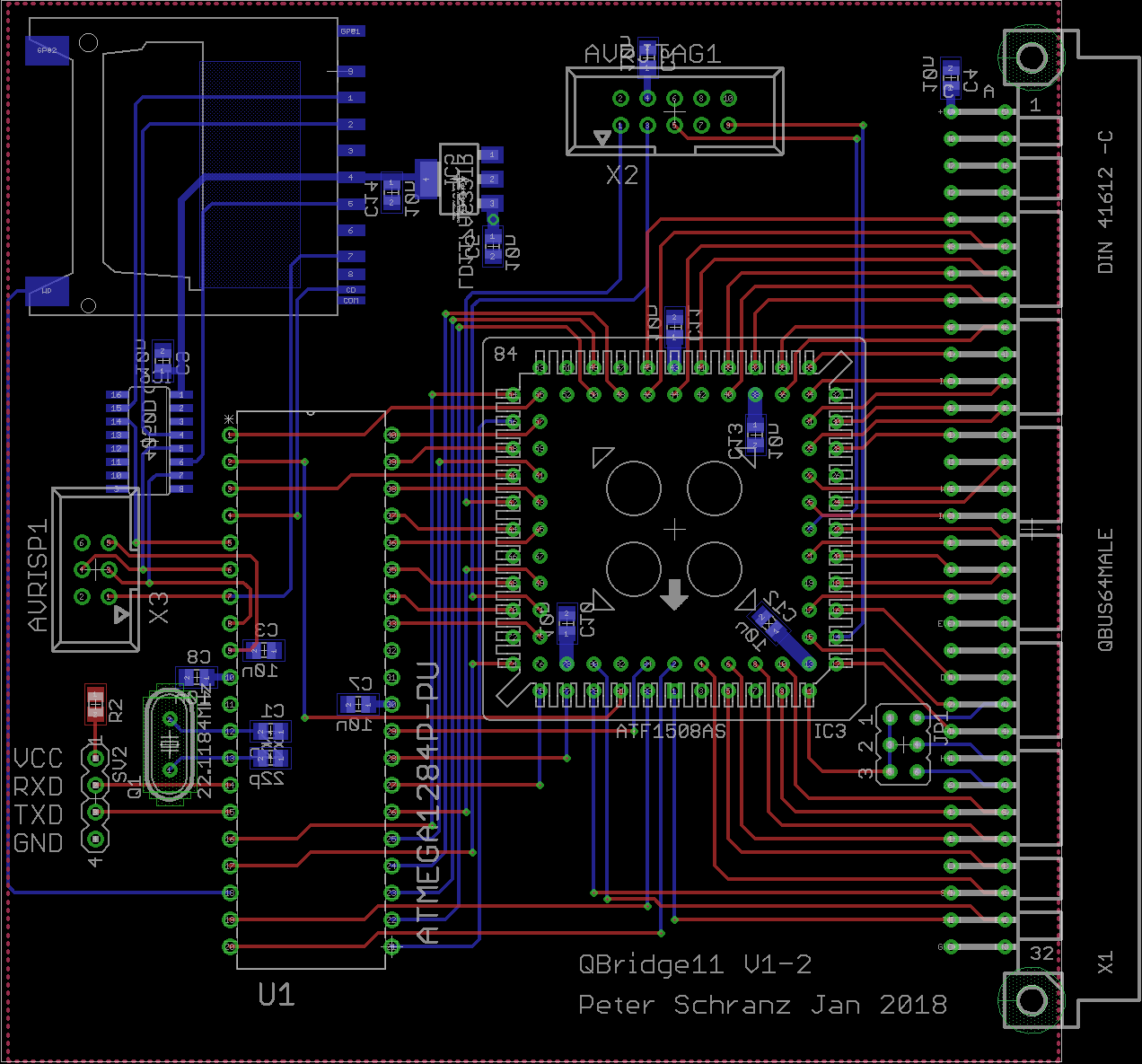
A description of the RLV12 emulator V2.0 can be found here.
First RLV12 Emulator for the PDP-11/Hack
Here are pictures of the first RLV12 Emulator with the decoupling capacitors added on the fly. You can also see a 2k2 pull-up resistor on the DO pin of the SD-Card slot. This is required as before the SD-Card interface is set to SPI the output is open collector and requires a pull-up resistor.
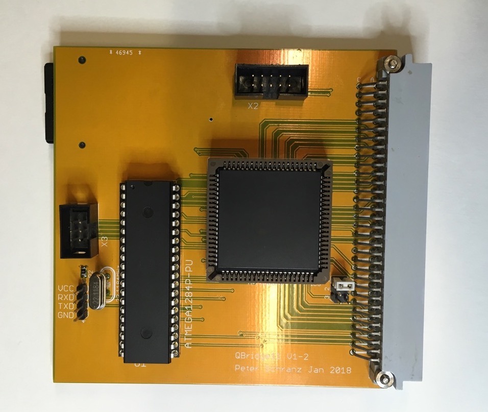
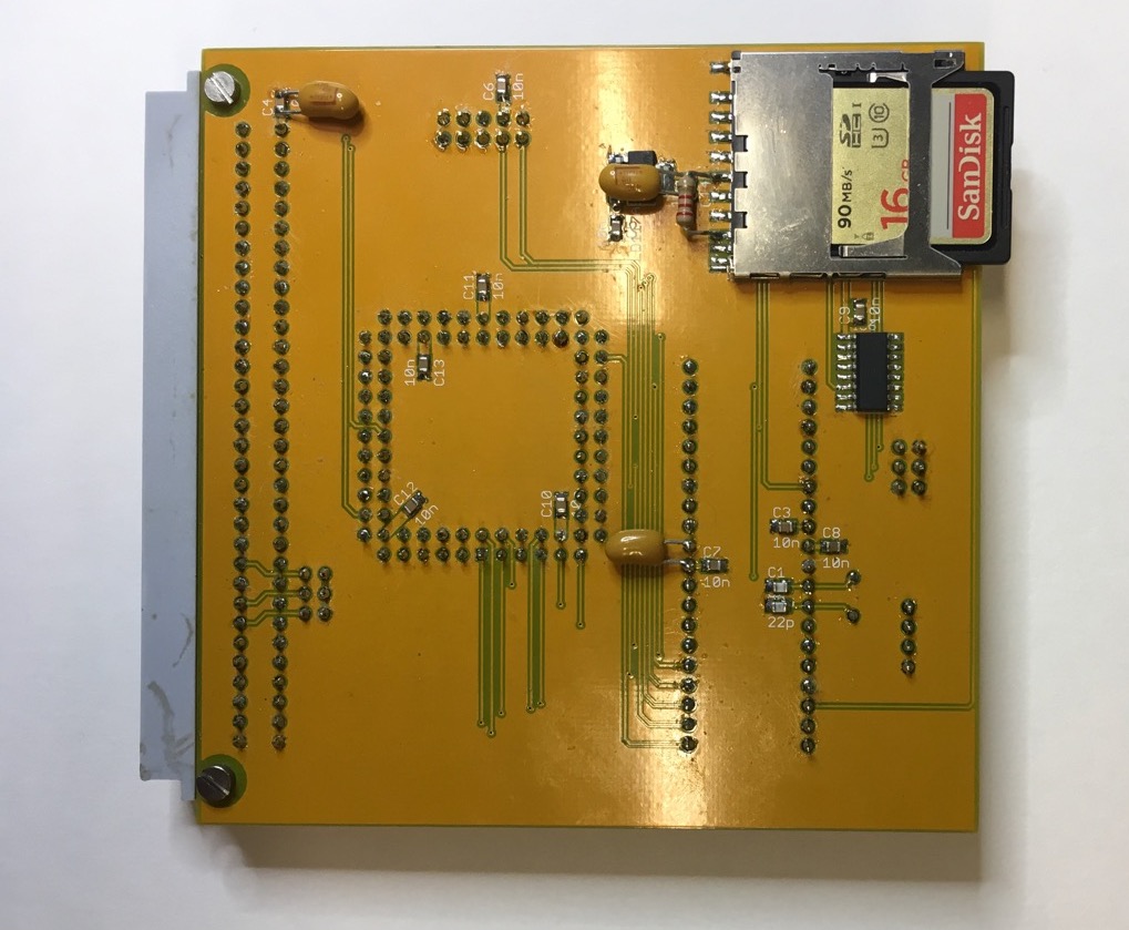
On the rear side you can see the added capacitors. In this picture the connections are as they were in the original state, in the meantime I have change some connections between the MCU and the CPLD to make better use special function inputs of the CPLD.
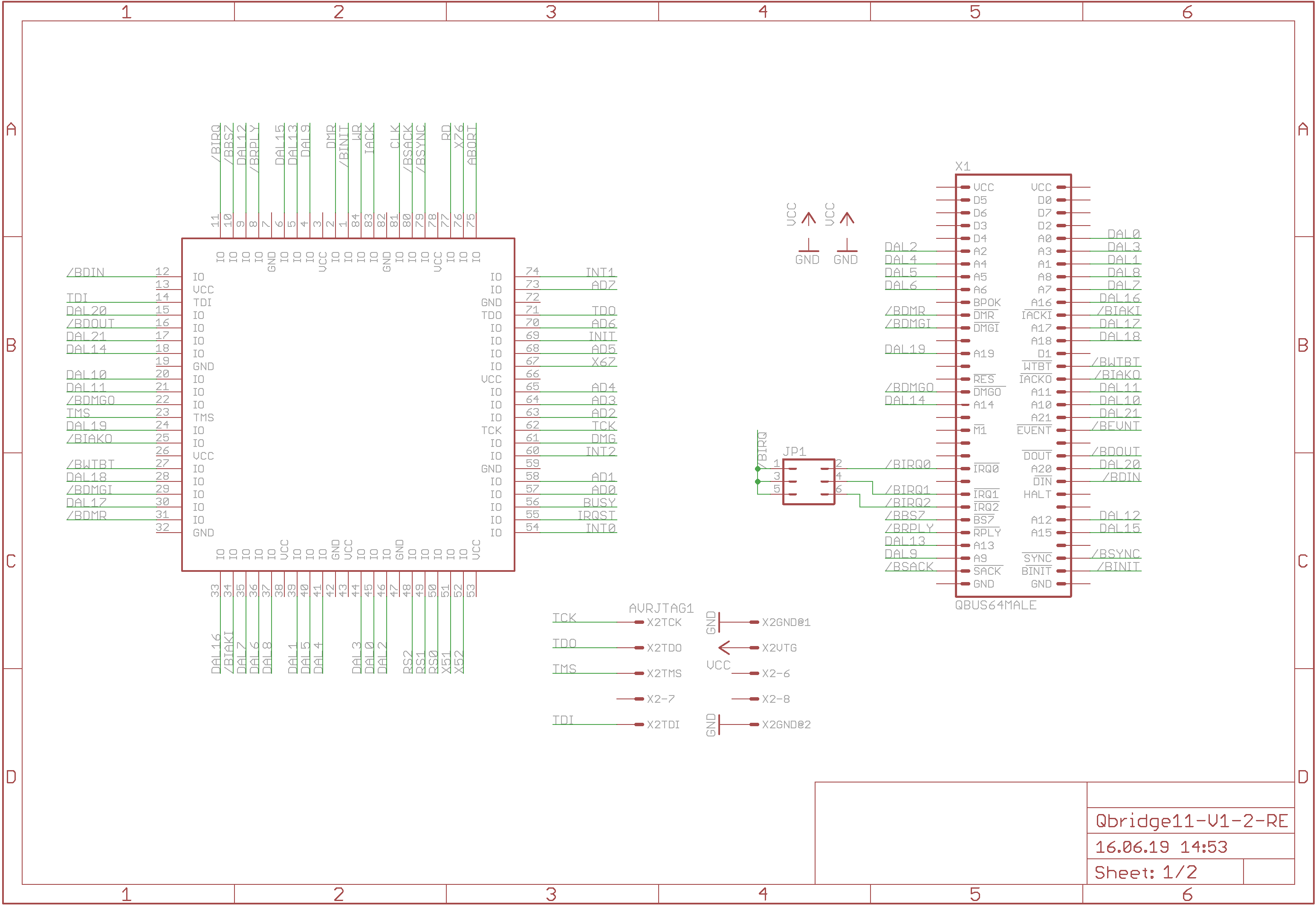
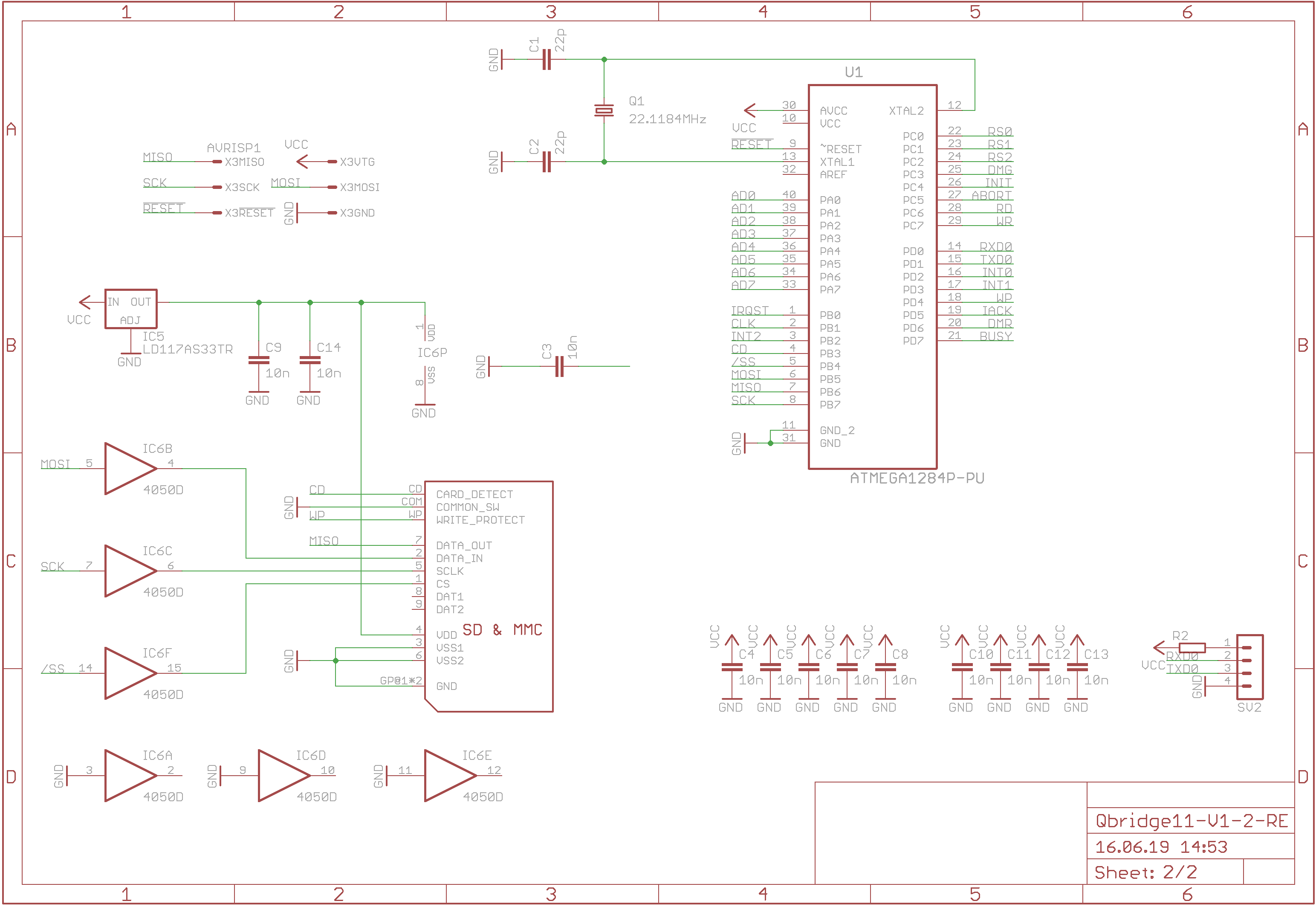
Schematic
Note the following are the schematics and boards as they are used in the prototype currently used in the PDP-11/Hack system. However there are some modifications required. First I forgot to add decoupling capacitors with 10µF to buffer the high current peak when inserting an SD-Card. This can cause a reset of the whole system. I added them on the fly to the board.
Also the Hack version connected a different pin of the microcontroller to the CLK1 input of the CPLD than the Q-Bus version. This has been ECO’d and now the same pin connects to CLK1 input on both RLV12 versions to have the same microcontroller program in both versions.
The change swaps pins 83 and 84 on the CPLD (cut the two traces and install two new wires)
CPLD Design
Name     Qbridge11-Mini ;
PartNo   01 ;
Date     05.12.2018 ;
Revision 01 ;
Designer cbscpe ;
Company  PRIVAT ;
Assembly None ;
Location ATHOME ;
Device   f1508ispplcc84 ;

/*
    2018-12-05  Based on the working RVL12 Emulator (See Qbridge11, v1) now
                with DMA implemented as state machine. The interface towards
                the MCU consists now only of 2 pins. A DMR (DMA Request) from
                the MCU and the DMG (DMA Grant) to the MCU to signal the
                progress and allows the MCU to read and write the DMA data
                using the normal data register. The DMA data register is gone.
                The Base Control Register CS1 is now implemented as an internal
                register. That is when reading CS1 then the internal register
                is immediately returned to the PDP-11 and the MCU is not interrupted.

    2018-12-12  Correct BDAL select signals, use positive logic for UB and LB, adapt
                the comments in the section to the new design, remove uneccessary PINNODE

    2018-12-19  New Statemachine concept

    2018-12-21  Additional cycles between SACK and SYNC and SYNC and data phase
                Bidirectional open collector signals must not be registered else WinCUPL
                will use the output of the flip-flop and not the PIN as input, sometimes
                you must even force equations

    2018-12-22  New PDP-11 interrupt logic. Now the MCU just sets IRQST when an interrupt
                is requested. This asserts BIRQ and on the next BDIN cycle the status is
                latched. In case we are the highest priority device when the interrupt
                is acknowledged by the PDP-11 the MCU is alerted via INT2. The MCU has
                then to take care of the various signals related to the interrupt. I.e.
                the MCU must de-assert IRQST and must clear the INT2 interrupt. If required
                the MCU can then also update the CS1 register. E.g. the RH70 always clears
                IE if an interrupt is acknowledged.
 */

$INCLUDE Z:\OneDrive\Dokumente\WinCupl\QBridge11-v2\Qbridge-11-v2-0-0.txt

PROPERTY ATMEL {SOFT_BUFFER=BUSEN};
PROPERTY ATMEL {preassign KEEP};
PROPERTY ATMEL {open_collector=BRPLY, BDMR, BSACK, BDOUT, BDIN, BSYNC, BRPLY, BWTBT};

PINNODE         =  [D15..0]      ; /* Data Output Register                                  */
PINNODE         =  [DD15..0]     ; /* DMA Data and Interrupt Vector Register                */
PINNODE         =  [A21..1]      ; /* DMA Address                                           */
PINNODE         =  [C5..0]       ; /* IO  Address                                           */
PINNODE         =  CSRADDR       ; /* CSR Address                                           */
PINNODE         =  CSR           ; /* CSR Address                                           */
PINNODE         =  CS1ADDR       ; /* CS1 Address                                           */
PINNODE         =  CS1           ; /* CS1 Address                                           */
PINNODE         =  [DMA4..0]     ; /*                                                       */
PINNODE         =  SYNC          ; /*                                                       */
PINNODE         =  DMGI          ; /*                                                       */
PINNODE         =  SACK          ; /*                                                       */
PINNODE         =  DATA          ; /*                                                       */
PINNODE         =  RPLY          ; /*                                                       */
PINNODE         =  DMARW         ; /*  Control bit: DMA read(1) or DMA write(0)             */
PINNODE         =  BUSEN         ; /*                                                       */
PINNODE         =  DIRQ          ; /* Device Interrupt Request                              */
PINNODE         =  DACK          ; /* Device Interrupt Acknowledge                          */
PINNODE         =  TDOUT;
PINNODE         =  TSYNC;
PINNODE         =  TDIN;


/*
    Define one of the possible emulations: RLV12, RH70
 */
$DEFINE RLV12

/*
    Field definitions
 */
FIELD  ADDR     = [C5..0];      /* Latched address used for register address                */
FIELD  RS       = [RS2..0];     /* Register Select Address for Atmega 162 reads/writes      */
FIELD  IOADDR   = [BDAL12..0];  /* Access to IO Page only requires address lines 0..12      */
FIELD  DMA      = [DMA4..0];    /* DMA State Machine                                        */
/*
    Address bits BDAL0..5 are latched for every bus cycle and made available to the MCU
    to identify the selected device register
 */
ADDR.d        =  [BDAL5..0].io;
ADDR.ck       =  BSYNC.io;

/*
    BINIT is propagated to the MCU via the INIT signal. This is a normal MCU input so
    we can use the pin change interrupt to take actions for both edges of BINIT.
 */
INIT          =  BINIT.io;

/*
    CSRADDR and CS1ADDR are asserted whenever the bus addresses a CSR or the first CSR
    respectively. These signals are used to latch the selected states into CSR and CS1.

    RLV12 addresses
 */
$IFDEF RLV12
CSRADDR       =  IOADDR.io:['o'174400..174417];
CS1ADDR       =  IOADDR.io:['o'174400..174401];
$ENDIF

/*
    RH70 addresses
 */
$IFDEF RH70
CSRADDR       =  IOADDR.io:['o'176702..176757];
CS1ADDR       =  IOADDR.io:['o'176700..176701];
$ENDIF

CSR.ck        =  BSYNC.io;
CSR.d         =               BBS7.io &  CSRADDR;

CS1.ck        =  BSYNC.io;
CS1.d         =               BBS7.io &  CS1ADDR;
/*
    DATI to a device register, except for CS1, triggers the INT1 interrupt. The first
    device register is implemented as local register and bus reads to this register
    are handeled in the CPLD. This allows us to always let the PDP-11 interrupt the MCU
    to support overlapped processing of register IO and data transfer/seek functions.
    CS1 is implemented as local register in order to avoid the MCU beeing permanently
    interrupted when the PDP-11 polls the controller instead of using interrupts.
    This is mainly the case during the boot phase.

    When the MCU has finished the processing the device register access it must create
    a pulse to IACK to acknowledge the interrupt and the CPLD then asserts BRPLY.
 */
INT1.d        = !(!BWTBT.io &  BBS7.io &  CSRADDR & !CS1ADDR);
INT1.ck       =  BSYNC.io;
INT1.ap       =  IACK;

/*
    DATO to a device register triggers INT0 interrupt.
 */
INT0.d        =  !(BWTBT.io &  BBS7.io &  CSRADDR);
INT0.ck       =  BSYNC.io;
INT0.ap       =  IACK;

BRPLY         =  CSR &  BSYNC.io &  INT1 &  BDIN.io       /* Assert RPLY when MCU is done   */
              #  CSR &  BSYNC.io &  INT0 &  BDOUT.io;     /* Assert RPLY when MCU is done   */

/*
    The interrupt logic is now fully handled in software so we can also update CS1 if needed.
    The CPU sets IRQST whenever an interrupt is required. This asserts !BIRQ on the QBUS. When
    the PDP-11 acknowledges the interrupt first DACK will be set which causes INT2 to be reset
    when !BIAKI is asserted. In the INT2_isr of the MCU the first action will be to deassert
    IRQST and then eventually update CS1. Then it will have to set INT2 in the CPLD with a
    short pulse on IACK which then asserts BRPLY.

           +----------------------------+
IRQST      |                            |
        ---+                            +------------------------------------------------

        ---+                            +------------------------------------------------
!BIRQ      |                            |
           +----------------------------+

        ----------+                                           +--------------------------
!BDIN             |                                           |
                  +-------------------------------------------+

    DACK This reflects always IRQST latched with BDIN as on all devices and therefore is
    only de-asserted on next falling edge of !BDIN
                   +---------------------------------------------------------------------
DACK               |
        -----------+

        -----------------+                                    +--------------------------
!BIAKI                   |                                    |
                         +------------------------------------+

                                             +---+
IACK                                         |   |
        -------------------------------------+   +---------------------------------------

        -----------------+                    +------------------------------------------
INT2                     |                    |
                         +--------------------+

        ---------------------------------------+               +-------------------------
!BRPLY                                         |               |
                                               +---------------+

 */
DACK.d        =  IRQST;
DACK.ck       = !DMA3     &  BDIN.io;
DACK.ar       =  BINIT.io;

BIAKO         =  BIAKI    & !DACK;
BIRQ          =  IRQST;

INT2.d        = !DACK;
INT2.ck       =  BIAKI;
INT2.ap       =  IACK;

APPEND
BRPLY         =  BIAKI & !IRQST &  INT2 & BDIN.io;

/*
    Q-Bus Data Register

 */
[D7..0].d     =  [AD7..0].io;
[D15..8].d    =  [AD7..0].io;
[D15..0].ck   =  WR;
[D7..0].ce    =  RS:['d'0];
[D15..8].ce   =  RS:['d'1];


/*
    Control and Status Register
 */
[DD7..0].d    =  [AD7..0].io;
[DD15..8].d   =  [AD7..0].io;
[DD15..0].ck  =  WR;
[DD7..0].ce   =  RS:['d'2];
[DD15..8].ce  =  RS:['d'3];


/*
    DMA Address
 */
DMARW.ar      =  WR  &  RS:['d'4] & !AD0.io;
DMARW.ap      =  WR  &  RS:['d'4] &  AD0.io;
DMARW.ck      = 'b'0;
DMARW.d       = 'b'0;

[A7..1].ar    =  WR  &  RS:['d'4] & ![AD7..1].io;
[A7..1].ap    =  WR  &  RS:['d'4] &  [AD7..1].io;

[A15..8].ar   =  WR  &  RS:['d'5] & ![AD7..0].io;
[A15..8].ap   =  WR  &  RS:['d'5] &  [AD7..0].io;

[A21..16].ar  =  WR  &  RS:['d'7] & ![AD5..0].io;
[A21..16].ap  =  WR  &  RS:['d'7] &  [AD5..0].io;

/*
    The MCU can read the 16-bit Q-Bus data using the two register address 0 and 1 for
    the even and odd byte respectively. Register address 4 contains the latched CSR
    offset together with two bits that indicate whether the upper or lower byte are
    written.

 */
UB            = !BWTBT.io
              #  BWTBT.io  &  C0;
LB            = !BWTBT.io
              #  BWTBT.io  & !C0;

[AD7..0]      =  RS:['d'0] &  [BDAL7..0].io
              #  RS:['d'1] &  [BDAL15..8].io
              #  RS:['d'4] &  [UB, LB, C0, C5, C4, C3, C2, C1];
/*
              #  RS:['d'4] &  [A7..1, DMARW]
              #  RS:['d'5] &  [A15..8]
              #  RS:['d'7] &  ['b'0, 'b'0, A21..16];
 */
[AD7..0].oe   =  RD;


/*
    Synchronous counter for DMA address which is updated after every DMA cycle. The address
    is incremented whenever a DMA cycle has finished.
 */
[A21..1].ck   = !DMA3;

A1.t          = 'b'1;
A2.t          = A1;
A3.t          = A1 & A2;
A4.t          = A1 & A2 & A3;
A5.t          = A1 & A2 & A3 & A4;
A6.t          = A1 & A2 & A3 & A4 & A5;
A7.t          = A1 & A2 & A3 & A4 & A5 & A6;
A8.t          = A1 & A2 & A3 & A4 & A5 & A6 & A7;
A9.t          = A1 & A2 & A3 & A4 & A5 & A6 & A7 & A8;
A10.t         = A1 & A2 & A3 & A4 & A5 & A6 & A7 & A8 & A9;
A11.t         = A1 & A2 & A3 & A4 & A5 & A6 & A7 & A8 & A9 & A10;
A12.t         = A1 & A2 & A3 & A4 & A5 & A6 & A7 & A8 & A9 & A10 & A11;
A13.t         = A1 & A2 & A3 & A4 & A5 & A6 & A7 & A8 & A9 & A10 & A11 & A12;
A14.t         = A1 & A2 & A3 & A4 & A5 & A6 & A7 & A8 & A9 & A10 & A11 & A12 & A13;
A15.t         = A1 & A2 & A3 & A4 & A5 & A6 & A7 & A8 & A9 & A10 & A11 & A12 & A13 & A14;
A16.t         = A1 & A2 & A3 & A4 & A5 & A6 & A7 & A8 & A9 & A10 & A11 & A12 & A13 & A14 & A15;
A17.t         = A1 & A2 & A3 & A4 & A5 & A6 & A7 & A8 & A9 & A10 & A11 & A12 & A13 & A14 & A15 & A16;
A18.t         = A1 & A2 & A3 & A4 & A5 & A6 & A7 & A8 & A9 & A10 & A11 & A12 & A13 & A14 & A15 & A16 & A17;
A19.t         = A1 & A2 & A3 & A4 & A5 & A6 & A7 & A8 & A9 & A10 & A11 & A12 & A13 & A14 & A15 & A16 & A17 & A18;
A20.t         = A1 & A2 & A3 & A4 & A5 & A6 & A7 & A8 & A9 & A10 & A11 & A12 & A13 & A14 & A15 & A16 & A17 & A18 & A19;
A21.t         = A1 & A2 & A3 & A4 & A5 & A6 & A7 & A8 & A9 & A10 & A11 & A12 & A13 & A14 & A15 & A16 & A17 & A18 & A19 & A20;


/*
    Q-Bus Output Select and Output Enable

    DMA4    DMA Read is active
    DMA3    DMA is active
    DMA2    DMA data transfer
 */
[BDAL15..0]   = !BIAKI & !DMA3  &  CS1   &  [DD15..0]
              # !BIAKI & !DMA3  & !CS1   &  [D15..0]
              # !BIAKI &  DMA3  & !DMA2  &  [A15..1, 'b'0]
              # !BIAKI &  DMA3  &  DMA2  &  [D15..0]
$IFDEF RLV12
              #  BIAKI                   &  [D15..0];
$ENDIF
$IFDEF RH70
              #  BIAKI                   &  'o'160;
              #  BIAKI                   &  'o'254;
$ENDIF

BUSEN         = !BIAKI          & !DMA3  &  CSR   &  BDIN.io &  BSYNC.io
              #  BIAKI          & !DMA3  &  DACK  &  BDIN.io
              # !BIAKI & !DMA4  &  DMA3                      /* 0x08..0x0F DMA Write   */
              # !BIAKI &  DMA4  &  DMA3  & !DMA2;            /* 0x18..0x1B DMA Read    */

/*
    The upper address bits are just a copy of the DMA address.
 */
[BDAL21..16]  =  [A21..16];
[BDAL21..0].oe=  BUSEN;
/*
    Partially CPLD controlled DMA state machine
 */

 /*
    The rising edge of DMR from the MCU triggers BDMR of the Q-Bus when
    the DMA is granted BDMR is cleared but DMR will be kept asserted by
    the MCU until the MCU has finished the DMA. Used to control the state
    machine.
  */
BDMR.d        = 'b'0;
BDMR.ck       =  DMR;
BDMR.ap       =  DMA3 # BINIT # ABORT;

TSYNC.ck      =  CLK;
TDOUT.ck      =  CLK;
TDIN.ck       =  CLK;
/*
    Synchronous Signals
 */
DMGI.ck       =  CLK;
DMA.ck        =  CLK;
RPLY.ck       =  CLK;
DMG.ck        =  CLK;

DMA.ar        =  BINIT.io # ABORT;
/*
    Latched BDMGI and BRPLY as we need a stable DMGI and RPLY for the state machine
 */
DMGI.d        =  BDMGI;
RPLY.d        =  BRPLY.io;


/*
    New DMA state machine.

    0. If signals are simultanuously configured as open collector, register and
    are used bidirectional WinCUPL unfortunately does not take the .PIN when we
    refer to .io extension. Therefore we cannot use the statemachine signals as
    open collector IO pins. Therefore we need additional signals TSYNC, TDOUT
    and TDIN.
    1. This state machine interacts directly with the MCU for the data transfer.
    First the MCU requests a DMA with a rising edge on DMR which asserts BDMR.
    When the CPU acknoweldges a DMA request it asserts BDMGI. This daisy chain
    signal must be propagated by all devices until it reaches the first that
    requested the DMA. In case we did not request the DMA (DMR is de-asserted)
    the statemachine will propagate BDMGI to BDMGO and wait until BDMGI is
    de-asserted and returns to the idle state. When we have requested the DMA
    the statemachine will assert BSACK, place the DMA address onto the data
    bus and then asserts BSYNC.
    2. For DMA writes the state machine then asserts DMG which is polled by the
    MCU which then loads the bus data register with the DMA data. Once the data
    has been written the MCU de-asserts DMR and the statemachine will finish
    the DMA write request.
    3. For DMA reads the the state machine waits for BRPLY to be asserted and
    will then assert DMG to signal the MCU that the DMA data can be read from
    the QBUS. Once the MCU has done this it will de-assert DMR and the state
    machine will finish the DMA cycle.
    4. DMG will be deasserted when the state machine has finished the DMA cycle.
    So before the MCU starts another DMA cycle it must check DMG to be de-asserted.

    Transfer rate is approximatively 1Mbyte/second and a DMA cycle takes about
    1usec. DMA on a real PDP-11 has about twice the performance, i.e. the transfer
    rate is about 2Mbyte/second and a DMA cycle only takes about 500ns. However
    the SD-Card has no seek and rotational latency. This more then compensates it.
 */

sequence DMA {

   PRESENT 'h'00 IF !DMGI                NEXT 'h'00;
                 IF  DMGI                NEXT 'h'01;

   PRESENT 'h'01 IF !DMR                 NEXT 'h'02;
                 IF  DMR                 NEXT 'h'03;

   PRESENT 'h'02 IF !DMGI                NEXT 'h'00;
                 IF  DMGI OUT BDMGO;     NEXT 'h'02;

   PRESENT 'h'03 IF !DMARW               NEXT 'h'08;
                 IF  DMARW               NEXT 'h'18;
/*
     Write
*/
   PRESENT 'h'08                         NEXT 'h'09           OUT DMG;

   PRESENT 'h'09                         NEXT 'h'0A           OUT DMG;

   PRESENT 'h'0A                         NEXT 'h'0B OUT TSYNC OUT DMG;

   PRESENT 'h'0B                         NEXT 'h'0C OUT TSYNC OUT DMG;

   PRESENT 'h'0C IF  DMR                 NEXT 'h'0C OUT TSYNC OUT DMG;
                 IF !DMR                 NEXT 'h'0D OUT TSYNC OUT DMG OUT TDOUT;

   PRESENT 'h'0D IF !RPLY                NEXT 'h'0D OUT TSYNC OUT DMG OUT TDOUT;
                 IF  RPLY                NEXT 'h'0E OUT TSYNC OUT DMG OUT TDOUT;

   PRESENT 'h'0E IF  RPLY                NEXT 'h'0E OUT TSYNC OUT DMG;
                 IF !RPLY                NEXT 'h'0F           OUT DMG;

   PRESENT 'h'0F                         NEXT 'h'00;
/*
     Read
*/
   PRESENT 'h'18                         NEXT 'h'19;

   PRESENT 'h'19                         NEXT 'h'1A;

   PRESENT 'h'1A                         NEXT 'h'1B OUT TSYNC;

   PRESENT 'h'1B                         NEXT 'h'1C OUT TSYNC;

   PRESENT 'h'1C IF !RPLY                NEXT 'h'1C OUT TSYNC         OUT TDIN;
                 IF  RPLY                NEXT 'h'1D OUT TSYNC OUT DMG OUT TDIN;

   PRESENT 'h'1D IF  DMR                 NEXT 'h'1D OUT TSYNC OUT DMG OUT TDIN;
                 IF !DMR                 NEXT 'h'1E OUT TSYNC OUT DMG;

   PRESENT 'h'1E IF  RPLY                NEXT 'h'1E OUT TSYNC OUT DMG;
                 IF !RPLY                NEXT 'h'1F           OUT DMG;

   PRESENT 'h'1F                         NEXT 'h'00;
}

BSACK         =          DMA3;
BWTBT         = !DMA4 &  DMA3 & !DMA2 & !DMA1;
BSYNC         =  DMA3 &  TSYNC;
BDOUT         =  DMA3 &  TDOUT;
BDIN          =  DMA3 &  TDIN;
The pin allocation definitions already reflects the ECO (swap of IACK and WR).
/* This is the workfile to change pin allocations

    2018-12-05  Based on the working RVL12 Emulator (See Qbridge11, v1) now
                with DMA implemented as state machine. The interface towards
                the MCU consists now only of 2 pins. A DMR (DMA Request) from
                the MCU and the DMG (DMA Grant) to the MCU to signal the
                progress.
    2018-12-28  Swap RD and IACK to keep changes to the real Q-Bus version minimal,
                i.e. only need to swap IACK and WR in the Atmega1284P definitions
    2018-07-03  Swap differently, just swap WR and IACK and keep RD on a sub-optimal
                input, this results in the same pin allocation of the MCU on both
                versions. RD should in fact go to a OE input pin to save product
                terms and fan-in, however the AD multiplexor is not at it's limit
                so it does still fit the CPLD.

*/

Device   f1508ispplcc84 ;

/*************************** Control Bus *******************************************************/
PIN    79  = !BSYNC          ; /* Address Latch Enable Transmit                           QBUS */
PIN     1  = !BINIT          ; /* Master reset                                            QBUS */
PIN    16  = !BDOUT          ; /* IO Bus write                                            QBUS */
PIN    34  = !BIAKI          ; /* Interrupt acknowledge daisy chain in                    QBUS */
PIN    11  = !BIRQ           ; /* Interrupt request                                       QBUS */
PIN    25  = !BIAKO          ; /* Interrupt acknowledge daisy chain out                   QBUS */

PIN    31  =  BDMR           ; /*                                                         QBUS */
PIN    29  = !BDMGI          ; /*                                                         QBUS */
PIN    22  = !BDMGO          ; /*                                                         QBUS */
PIN    80  = !BSACK          ; /*                                                         QBUS */

PIN    12  = !BDIN           ; /* IO Bus read                                             QBUS */
PIN    27  = !BWTBT          ; /* Multiplexed Write/Byte                                  QBUS */
PIN    10  = !BBS7           ; /* Bank Select 7 i.e. registers in IO page                 QBUS */
PIN     8  = !BRPLY          ; /* Continue daisy chain in                                 QBUS */

/*************************** Address/Data Bus **************************************************/
PIN    45  =  BDAL0           ; /*                                                         QBUS */
PIN    39  =  BDAL1           ; /*                                                         QBUS */
PIN    46  =  BDAL2           ; /*                                                         QBUS */
PIN    44  =  BDAL3           ; /*                                                         QBUS */
PIN    41  =  BDAL4           ; /*                                                         QBUS */
PIN    40  =  BDAL5           ; /*                                                         QBUS */
PIN    36  =  BDAL6           ; /*                                                         QBUS */
PIN    35  =  BDAL7           ; /*                                                         QBUS */
PIN    37  =  BDAL8           ; /*                                                         QBUS */
PIN     4  =  BDAL9           ; /*                                                         QBUS */
PIN    20  =  BDAL10          ; /*                                                         QBUS */
PIN    21  =  BDAL11          ; /*                                                         QBUS */
PIN     9  =  BDAL12          ; /*                                                         QBUS */
PIN     5  =  BDAL13          ; /*                                                         QBUS */
PIN    18  =  BDAL14          ; /*                                                         QBUS */
PIN     6  =  BDAL15          ; /*                                                         QBUS */
PIN    33  =  BDAL16          ; /*                                                         QBUS */
PIN    30  =  BDAL17          ; /*                                                         QBUS */
PIN    28  =  BDAL18          ; /*                                                         QBUS */
PIN    24  =  BDAL19          ; /*                                                         QBUS */
PIN    15  =  BDAL20          ; /*                                                         QBUS */
PIN    17  =  BDAL21          ; /*                                                         QBUS */

/*************************** AVR Interface *****************************************************/
PIN    81  =  CLK            ; /* Master Clock                                     Atmega1248P */

PIN    57  =  AD0            ; /* MCU <-> CPLD Data                                Atmega1248P */
PIN    58  =  AD1            ; /* "                                                Atmega1248P */
PIN    63  =  AD2            ; /* "                                                Atmega1248P */
PIN    64  =  AD3            ; /* "                                                Atmega1248P */
PIN    65  =  AD4            ; /* "                                                Atmega1248P */
PIN    68  =  AD5            ; /* "                                                Atmega1248P */
PIN    70  =  AD6            ; /* "                                                Atmega1248P */
PIN    73  =  AD7            ; /* "                                                Atmega1248P */
PIN    54  =  INT0           ; /* DATO Interrupt                                   Atmega1248P */
PIN    74  =  INT1           ; /* DATI Interrupt                                   Atmega1248P */
PIN    50  =  RS0            ; /* Register Select 0                                Atmega1248P */
PIN    49  =  RS1            ; /* Register Select 1                                Atmega1248P */
PIN    48  =  RS2            ; /* Register Select 2                                Atmega1248P */
PIN    84  =  IACK           ; /* Acknowledge CPDL Interrupts                      Atmega1248P */
PIN    83  =  WR             ; /* Write Register                                   Atmega1248P */
PIN    77  =  RD             ; /* AD Output Enable                                 Atmega1248P */
PIN    60  =  INT2           ; /* Interrupt Acknowledge                            Atmega1248P */
PIN    55  =  IRQST          ; /* Start Interrupt Request Cycle pulse              Atmega1284P */
PIN    69  =  INIT           ; /* Propagate BINIT (Pin Change Interrupt)           Atmega1248P */
PIN    75  =  ABORT          ; /* Abort DMA cycle (bus timeout)                    Atmega1248P */

/*************************** DMA Signals *******************************************************/
PIN     2  =  DMR            ; /* DMA Request                                      Atmega1248P */
PIN    61  =  DMG            ; /* DMA Grant                                        Atmega1248P */

/*************************** Previous interface Pins *******************************************/
/*     69  =  RPLY           ; /* BUS Reply                                        Atmega1248P */
/*     61  =  DMGI           ; /* DMA Grant Input                                  Atmega1248P */
/*      2  =  SACK           ; /* Service Acknowledge                              Atmega1248P */
/*     83  =  DMR            ; /* DMA Request                                      Atmega1248P */
MCU Software
The PDP-11/Hack version of the RLV12 emulator uses the same code as the Q-Bus version. You can find the software in the download section and some description in the RLV12 Emulator section