CPU Board with Memory
CPU Board Setup
The CPU board is built using a DCJ11 processor. To get the maximum performance it includes memory, that is the CPU must not access the system bus to read or write to the main memory. By using fast SRAM memory read cycles perform at the maximum speed, equivalent to a cache hit. In other words we do not need a cache memory as the whole memory is as fast as a cache memory can be for a DCJ11.
The CPU board is quite simple. It consists of the DCJ11, address latches, bus transceivers and SRAM. The SRAM are AS6C8016, 512k x 16bit. Currently only 1Mbyte is installed but you can install a second IC to get 2Mbyte of RAM
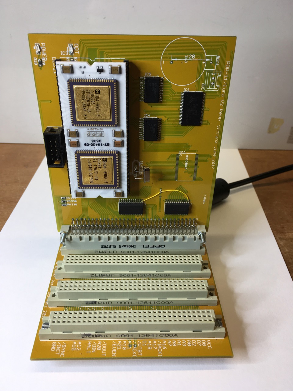
You can see a small engineering change which was due to some carelessness. Surprisingly enough it was the only modification required so far.
All the glue logic has been placed into a single ATF1508 CPLD which is located below the DCJ11 as you can see on the next picture. You will notice that this picture was taken before I applied the engineering change
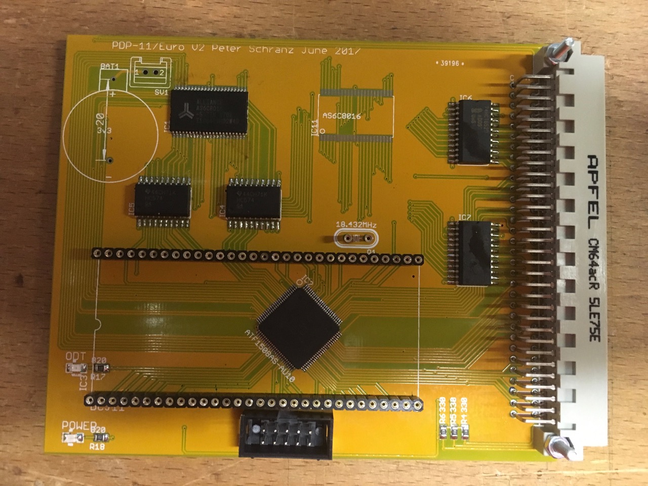
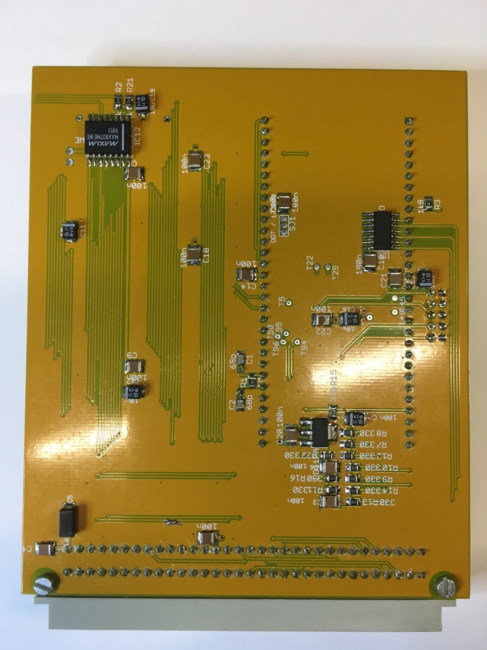
The next picture shows the back side of the CPU board, which shows the microcontroller supervisor, the inverters required for the interrupt lines and the 3V3 regulator and the pull-up resistors for the open collector signals
Schematic
The whole CPU board is surprisingly simple mostly due to the fact that the DCJ11 as a processor implements most functions directly and requires only little interface logic.
The first page contains the latch for the lower address bits (IC4 and IC5) the Memory and the bus transceivers for the lower 16 address/data bits. The transceivers use the 74HCT652 bidirectional bus transceivers with latch. This comes very handy to multiplex address and data on the bus.
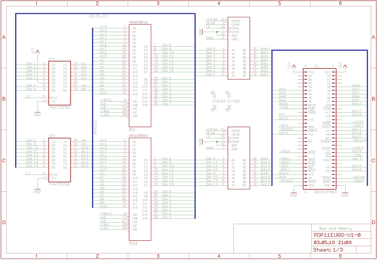
The second page just shows the DCJ11 and the CPLD
On the third page are miscellaneous parts like blocking capacitors, supervisor chip the termination for the open collector signals and the inverters for the interrupt request lines as the DCJ11 uses positive logic for the interrupt inputs.
As you can see nothing spectacular and quite simple.
Understanding the DCJ11
CPU Clock
The DCJ-11 has a built-in crystal oscillator which defines the time of a clock cycle. The -AC version is specified for a maximum clock of approximatively 15MHz, while the -AA version is specified for a maximum clock of approximatively 18MHz. Each bus cycle takes an even number of clock cycles. In my case I’m using a 22.1184MHz baud-rate crystal and all DCJ11 chips I have seem to be ok with this overclocking no matter of the type code. In the following I always refer to clock cycles for the basci crystal clock cycles and to CPU cycles for a a set of clock cycles used by the CPU to form a complete CPU cycle.
DCJ11 signals
The DCJ11 has a lot of multiplexed signals. The following signals change during the CPU cycle and should be latched using the ALE signal. You can either use transparent latches or D-type latches. Transparent latches have the advantage that the addresses are available earlier which might by an advantage when the timing for memory is tight, however SRAM today are very fast and it doesn’t matter. On the breadboard I was using 74HCT574 D-Type latches and used an inverted ALE signal to latch the signals. Later I kept using D-Type latches for almost everything. The following signals are very important for system control
Note that all these signals have a different meaning during the first and the second half of a CPU cycle.
Address Input/Output
In the first part of the CPU cycles AIO0..3 define the type of the Bus Cycle.
| AIO Code | Description | |||
|---|---|---|---|---|
| 1 | 1 | 1 | 1 | NIO — Non‐IO or internal CPU cycle, the CPU does not access the bus |
| 1 | 1 | 1 | 0 | GP READ — General Purpose Read |
| 1 | 1 | 0 | 1 | IACK — Interrupt Acknowledge Cycle |
| 1 | 1 | 0 | 0 | Instruction read |
| 1 | 0 | 1 | 1 | READ-MODIFY-WRITE no bus lock |
| 1 | 0 | 1 | 0 | READ-MODIFY-WRITE bus lock |
| 1 | 0 | 0 | 1 | Data Read |
| 1 | 0 | 0 | 0 | Demand Read |
| 0 | 1 | 0 | 1 | GP WRITE — General Purpose Write |
| 0 | 0 | 1 | 1 | Write Byte |
| 0 | 0 | 0 | 1 | Write Word |
Bank Select
The total address space of a DCJ-11 is split into different banks. Note that this does not extend the address space. You still have only 22 bit addresses. During the first part of the CPU cycle they indicate what type of memory location is accessed.
| Bank Select | Description | |
|---|---|---|
| 1 | 1 | Internal register |
| 1 | 0 | External I/O device |
| 0 | 1 | System register |
| 0 | 0 | Memory |
During the second half the signal are used to indiciate “force cache miss” and “force cache bypass”. In my design they are not honored.
MAP
In the first part of the CPU cycle MAP is asserted if the UNIBUS Map bit has been set in the memory management control register (Bit 5 of MMR3). This is required in systems with a UNIBUS Map in order to be able to activate or deactivate the UNIBUS Map. In the second part of the CPU cycle it is asserted if the CPU has honored a DMA request.
CPU Cycles
The DCJ11 differentiates between stretched and non-stretched cycles. Some CPU cycles are non-stretched and some are stretched by default. A non-stretched CPU cycle is exactly 4 clock cycles. The NON-IO and most Memory Read cycles are by default non-stretched. These cycles will be turned into a stretched cycle under certain circumstances.
The most basic cycle is a NON-IO non-stretched cycle. This cycle is used when the CPU performs internal operations and no bus access is performed
You read often that the DCJ11 supports a clock of 4.5MHz. However this rate refers to the maximum rate of CPU cycles when using a 18MHz quartz as the clock source. The 4.5MHz rather defines the maximum number of CPU cycles if all cycles are non-stretched.
NON-IO cycles will be stretched if DMR of the DCJ-11 has been asserted.
Memory read cycles will be stretched if either MISS or DMR of the DCJ-11 has been
asserted or if the instruction requires a read-modify-write cycle with bus lock.
Stretched cycles take at least 8 clock cycles. However they are only finished if
CONT of the DCJ-11 is asserted. This signal is sampled with the falling edge of
the T4 clock. If it is not asserted the CPU cycle will add another two T4
cycles until CONT is asserted.
All other cycles are stretched CPU cycles, that is they take at least 8 clock
cycles and require CONTto be asserted to finish.
CONT in conjunction with ABORT is used to signal a non-existing memory
location to the CPU. E.g. if the GLUE logic decides that the CPU has accessed a
non-existing memory or device address it will first assert ABORT and then
inform the CPU to continue by asserting CONT. The CPU will then trap through
vector 4(8). Bits 4 and 5 of the CPU Error Register at 17777766(8)
will give more information about the reason the CPU cycle was aborted.
Read-Modify-Write Cycles
There is no atomic read-modify-write cycle. All these cycles are split into a read, a potential NON-IO and a write cycle. However the read cycles that are part of a read-modify-write instruction that act on a memory location are marked as being part of a read-modify-write cycle.
Some instructions use a read-modify-write cycle with bus lock. These read
cycles are always stretched and bypass the cache. This may be used by
multi-CPU systems to lock out bus access of other CPUs to assure integrity of
memory locations in case multiple CPUs want to access the same location. There
are only a few instructions that make use if this read-modify-write with bus
lock cycles, like ASRB, WRTLCK and TSTSET. All other instructions use
simple read-modify
DMA
On every CPU cycle the DCJ11 checks the DMR input signal. The DCJ11 does not
perform the DMA itself it just propagates this signal in the second part of a
CPU cycle via the MAP output. Also the only thing the DCJ11 does on a DMA
request is turn non-stretched cycles into stretched cycles. It is then the task
of the external logic to provide the necessary support for a DMA request. The
external logic does not have to respond to DMA requests. The only consequence of
this is that DMR will probably not be de-asserted and the DCJ11 will again
signal a pending DMA request on the next CPU cycle.
For example the PDP-11/Hack only performs a DMA during a NON-IO or a memory read cycle. Because the CPU releases the address/data bus during these cycles I do not need additional buffers between the CPU and the memory and also the statemachine that handles DMA is much simpler.
CPDL Design File
The most sophisticated part of the CPU board are the design equations of the CPLD. In this chapter I will go a little bit firther into the parts which are not obvious.
Bus Time-Out
Like the real Q-Bus the CPU waits for the device or memory to respond and the cycle
is aborted when there is no response within 10µs. In fact the DCJ11 would wait
forever unless CONT is asserted.
The bus time-out is implemented as a counter, and not as a one-shot as it is on many
CPU boards. I use a 8-bit synchronous counter. The clock is the CPU clock and the
counter is held in reset state when STRB is not asserted. The DCJ11 asserts STRB to
signal an active CPU cycle.
When the counter reaches a count of 192 it will assert ABORT and finish the cycle
by asserting CONT. The DCJ11 will then execute an exception with the vector
stored at address 4(8).
COUNT.ck   =  CLK;
COUNT.ar   = !STRB;

SEQUENCED COUNT {
   $REPEAT i = [0..254]
   PRESENT 'd'{i} NEXT 'd'{(i+1)};
   $REPEND
   PRESENT 'd'255 NEXT 'd'255;
   }


ABORT      =  COUNT:['h'C0..FF]; /* Time-out after 192 clock cycles */


CONT       =
           .
           .
           #           COUNT:['h'C0..FF] &  SCTL
           .
           .
The exact time-out is not important, here it will of course change with the CPU clock but in general that is ok.
Data Valid
Another special input to the DCJ11 is the DV (data valid) input. On read cycles the DCJ11 assumes that the value is valid at the leading edge of T3 and latches the current value into the internal data register. However in case the source is not ready with it’s data at the leading edge of T3 the data latched will not be correct. For example if the CPU needs to access the bus, or in case of a cache miss, the data will only be available at a later stage. Generally when we have a stretched cycle data was not ready at that time. Therefore the DCJ11 provides DV to signal that the data is now ready, that means when DV is asserted the data is latched again and overwrites the previously loaded data.
Complete CPLD Source
I typically separate the PIN list with from the design file. During the PCB layout I will often change the PIN numbers in order to simplify signal routing. I also left all the comments which shows a little bit of how I was slowly learning to use CPLDs with this project.
Name PDP11EURO-V1-0 ;
PartNo 00 ;
Date 30.05.2017 ;
Revision 01 ;
Designer cbscpe ;
Company PRIVAT ;
Assembly None ;
Location Switzerland ;
Device f1508isptqfp100 ;
PROPERTY ATMEL {preassign = KEEP};
PROPERTY ATMEL {open_collector=ABORT, BRPLY, BDIN, BSYNC, BDOUT, BWTBT, BBS7, BINIT};
$INCLUDE C:\Wincupl\WinCupl\PDP11EURO\PDP11EURO-V1-0-0.txt
/*$DEFINE 2MB /* if we have 2 Mbyte installed, else do not define 2MB */
/*
GLUE logic for a DCJ11
======================
History
This is a fresh start of the big PDP-11 designs (PDP11SYS series). It has shown that a ATF1508AS
in a PLCC-84 package does not have enough pins to implement all features required for a full
fledge CPU board. Either we need an additional ATF1504AS and put the GPREAD and GPWRITE decoding
into the additional CPLD or we use a ATF1508AS in a TQFP-100 package. The number of macrocells
is sufficient as the logic itself is quite simple.
2017-06-05 Signals used as clock inputs
It is very important that signals used as clock for CPLD flip-flops are clearly
defined. Therefore all signals that come from the bus require a flip-flop that
catches the signal via a known clock (e.g. CLK or ALE), this is especially the case
for BRPLY, BEVENT and BPOK.
OPEN POINT: what happens with the DMA address latched with BSYNC.io? Probably this
is not an issue as they are not used for states but only for memory which is
asynchronous, just need to make sure that the address latches are happy with it.
Perhaps we will use latches (.le, .l) instead of D-FF (.ck, .d)
2017-06-10 Change of Memory Interface
Due to the fact that the 16-bit wide memory requires upper and lower byte enable
signals and that the MAX807 supervisor interface has only one CE gate, the logic to
select memory has been changed. We have now only one MREQ signal and individual byte
enable signals. As UB and LB require too much PTs I have decided to latch the state
for writing lower or upper byte, as well as the read state, from the AIO code into
latches to save product terms for the individual byte selects. This has no influence
to the acces time requirements of the memory as the state is latched with the falling
edge of /ALE. So these signals are valid about 40ns before /BUFCTL or /SCTL are
asserted which are used for the enable signals. This reduces the PTs required for LB0,
LB1, UB0 and UB1 to 5 each. The new latched cycle type signals and the reduction of
PTs makes it possible to route the byte select signals to every output.
2017-06-13 There is a huge advantage to use only 5 PTs for output signals, you can then place
them at any pin. Output signals with more than 5 PTs use a cascaded cell per default
to borrow those PTs. This makes the neighboring cell unusable and if it is associated
with a PIN you can use this PIN only as an input. CONT is the only output signal that
requires more than 5 PTs, in our case it requires 11 PTs and as there are no MC with
more than one free MC as a neighbor the neighbor PIN cannot be used as output. In our
case CONT is pin 92, the neighbor MC 15 has no pin associated but the next MC 14
is associated with pin 93. As we require 11 PTs both MC15 and MC14 are used to borrow
PTs for the MC16 of CONT. Note that the neighbor MCs must be from the same block, MC16
is the last MC of block A there are no restrictions. The first MC of a block cannot
borrow PTs as it has no upstream neighbor and the second MC can only borrow from the
first MC and so on. Note that you can borrow PTs from up to 7 neighbors to allow for
up to 40 PTs.
2017-07-22 PCB Board Version 1-0 has been ordered and arrived, no more PIN moves!
Todo
Rename all bus signals to the real Q-Bus names to be consistent with real Q-Bus
BRPLY, BDIN, BDOUT, BSYNC, BPOK, , BIAKO (IACKO), BDMGO (GRANT), BBS7, BWTBT
2017-08-03 Renaming done
2017-08-10 The last full version has been saved under the name PDP11EURO-V1-0-final.pld. The
file PDP11EURO-V1-0.pld will start only with the equations required to achieve feature
parity with MINI-11. Once this has been done we will successively add the DMA support.
2017-08-11 Correction use BS0 and BS1 for the latched cycle stats (AIOREAD, et.al.) and not LBS0 and LBS1
2017-08-12 IACK cycle needs to activate the 74HCT651/2 as well else the vector will not be read
2017-08-15 Clean-up (after also fixing bad solder contacts), now it boots RT11XM.
2017-08-19 Add DMA state machine without memory access
2017-09-09 DMA state machine seems to work
add memory access for lower 64kb RAM
2017-09-10 Fix errors and design flaws in some of the DMA related equations
BSYNC needs to be qualified with DMAACT else WinCUPL will collapse BSYNC.io and SYNC which
does not provide the desired result (e.g. BRPLY would never be asserted on DMA)
Use the transparent LATCH function for storing AD21..16, AD0, it is the way that seems
to be most adequate for the QBUS. For AD15..1 we still need to create a rising edge
for the 74HCT574 (signal LE), perhaps we should consider to use transparent latches
like the 74HCT573 in a next design.
DMA read/write words work as planned
2018-01-28 It seems I have screwed the last source code. The Jedec File loaded in the CPLD with
the version that perfectly boots RT-11 does not match the one created with the last
source code. Therefore I went back to the source code date from the 11th of september.
Not exactly the last version but at least very similar in behaviour.
2018-03-18 V1-1 Add Maintenance Register so RT-11 thinks this is a 11/73A
2018-03-23 Cycles with AIO Code 'b'1010, "Read-Modify-Write with bus-lock", are stretched cycles and
therefore require CONT to finish. Add product term that asserts CONT for such cycles and
valid memory addresses. Else a ASRB would time-out and generate a non-existant memory trap.
2018-08-02 !!!!!!!!!!!!!!!!!!!!!!!!!!!!!!!!!!!!!!!!!!!!!!!!!!!!!!!!!!!!!!!!!!!!!!!!!!!!!!!!!!!!!!!!!!
!!!!!!!!!!!!!!!!!!!!!!!!!!!!! DO NOT CHANGE DO NOT CHANGE !!!!!!!!!!!!!!!!!!!!!!!!!!!!!!!!
!!!!!!!!!!!!!!!!!!!!!!!!!!!!!!!!!!!!!!!!!!!!!!!!!!!!!!!!!!!!!!!!!!!!!!!!!!!!!!!!!!!!!!!!!!
The version loaded to the CPU board did not match this design. The CPLD code has been
saved to PDP11EURO-V1-1-2018-08-02.jed and a new version with this design file with
option 2MB deactivated has been loaded to the CPU board and was verified to boot RT-11
V5.7 and RSX-11Mplus 4.6 BL87.
*/
/*
Internal Signals
*/
/* */
PINNODE = SYNC ; /* Internal BSYNC generated for Q-Bus cycles, propagated to BSYNC */
PINNODE = DMAACT ; /* Set when a DMA is active and reset by STRB, used as MUX control */
PINNODE = LAIO0 ; /* */
PINNODE = LAIO1 ; /* */
PINNODE = LAIO2 ; /* */
PINNODE = LAIO3 ; /* */
PINNODE = LBS0 ; /* */
PINNODE = LBS1 ; /* */
PINNODE = A16 ; /* Latched Address Bit 16 for Memory */
PINNODE = A17 ; /* Latched Address Bit 17 for Memory */
PINNODE = A18 ; /* Latched Address Bit 18 for Memory */
PINNODE = A19 ; /* Latched Address Bit 19 for Memory */
PINNODE = A20 ; /* Latched Address Bit 20 for Memory */
PINNODE = A21 ; /* Latched Address Bit 21 for Memory */
PINNODE = AD0 ; /* Latched DMA Address Bit 0 for byte access */
PINNODE = AD16 ; /* Latched DMA Address Bit 16 for Memory */
PINNODE = AD17 ; /* Latched DMA Address Bit 17 for Memory */
PINNODE = AD18 ; /* Latched DMA Address Bit 18 for Memory */
PINNODE = AD19 ; /* Latched DMA Address Bit 19 for Memory */
PINNODE = AD20 ; /* Latched DMA Address Bit 20 for Memory */
PINNODE = AD21 ; /* Latched DMA Address Bit 21 for Memory */
PINNODE = CNT0 ; /* 8-bit counter that counts the number of clock cycles passed */
PINNODE = CNT1 ; /* in a read or write cycle, started when a cycle is active, i.e. */
PINNODE = CNT2 ; /* !STRB is asserted and used as timeout when no BRPLY has been */
PINNODE = CNT3 ; /* received after a given number of clock cycles */
PINNODE = CNT4 ; /* */
PINNODE = CNT5 ; /* */
PINNODE = CNT6 ; /* */
PINNODE = CNT7 ; /* */
PINNODE = QBUS0 ; /* Q-Bus statemachine */
PINNODE = QBUS1 ; /* " */
PINNODE = QBUS2 ; /* " */
PINNODE = DIO ; /* Data IO phase */
PINNODE = ADD ; /* Address out phase */
PINNODE = DMA0 ; /* DMA statemachine */
PINNODE = DMA1 ; /* " */
PINNODE = DMA2 ; /* " */
PINNODE = DMG ; /* Accept grant from CPU */
PINNODE = IACK0 ; /* IACK statemachine */
PINNODE = IACK1 ; /* " */
PINNODE = IACK2 ; /* " */
PINNODE = DINACK ; /* DIN for Interrupt ACK */
/*
Asynchronous signals that must be synced to a clock before they can be used
*/
PINNODE = RPLY ; /* Internal BRPLY synced with CLK for statemachine */
PINNODE = SACK ; /* Internal BSACK synced with CLK for statemachine */
PINNODE = LEVENT ; /* Latched BEVENT to avoid race condition */
PINNODE = LPF ; /* Latched Power fail to avoid race condition */
PINNODE = LPOK ; /* Latched Power OK */
/*
For simpler routing and placement and to save PTs for otherwise complex equations we latch
some AIO codes in dedicated status latches. Especially memory reads and writes which use
multiple AIO codes. This has no speed penalty as they are all valid with ALE like the latched
AIO lines that would otherwise be used for the equations.
*/
PINNODE = AIOWRITEL ; /* AIO latched for memory writes that update lower byte */
PINNODE = AIOWRITEU ; /* AIO latched for memory writes that update upper byte */
PINNODE = AIOREAD ; /* AIO latched for memory reads */
PINNODE = POWERUP ; /* GPREAD code = read power up register */
PINNODE = ASSEVENT ; /* GPWRITE code = assert event (latched) */
PINNODE = ASSPWRF ; /* GPWRITE code = assert power fail (latched) */
/*
*/
PINNODE = MAINT ; /* Maintenance Register 17'777'750 */
PINNODE = CCR ; /* Cache Control Register 17'777,746 */
/*
Field Definitions
*/
FIELD COUNT = [CNT7..0];
FIELD QBUS = [QBUS2..0];
FIELD IACK = [IACK2..0];
FIELD DMA = [DMA2..0];
FIELD ADDRESS = [A7..0];
/*
General Latch Enable Signal for edge triggered latches like the 74HCT574, 74HCT651/2
*/
LE = ALE & !STRB
# BSYNC.io & DMAACT;
/*
The CPU asserts ALE for all time multiplexed signals, so we need to latch them with the leading
edge of ALE (note ALE is active low which means electrically the falling edge of the CPU signal).
To save product terms we also latch complete combinatorial states for memory access cycles.
AIO3 AIO2 AIO1 AIO0 Cycle
1 1 1 1 NIO
1 1 1 0 GPREAD
1 1 0 1 IACK
1 1 0 0 Instruction Stream Read
1 0 x x Read
0 1 0 1 GPWRITE
0 0 1 1 Byte Write
0 0 0 1 Word Write
BS1 BS0 Region
1 1 Internal Register
1 0 I/O Register
0 1 System Register
0 0 Memory
*/
[LAIO3..0, LBS1..0].d = [AIO3..0, BS1..0];
[LAIO3..0, LBS1..0].ck = ALE;
AIOWRITEL.d = !AIO3 & !AIO2 & !AIO1 & AIO0 & !BS1 & !BS0
# !AIO3 & !AIO2 & AIO1 & AIO0 & !BS1 & !BS0 & !DAL0.io;
AIOWRITEL.ck = ALE;
AIOWRITEU.d = !AIO3 & !AIO2 & !AIO1 & AIO0 & !BS1 & !BS0
# !AIO3 & !AIO2 & AIO1 & AIO0 & !BS1 & !BS0 & DAL0.io;
AIOWRITEU.ck = ALE;
AIOREAD.d = AIO3 & AIO2 & !AIO1 & !AIO0 & !BS1 & !BS0
# AIO3 & !AIO2 & !BS1 & !BS0;
AIOREAD.ck = ALE;
/*
The latches external to the CPLD only latch address bits DAL1..DAL15, or in case of DMA the address
bits BA15..1, the CPLD takes care of the higher address bits DAL21..16 and in case of DMA the DMA
address bits BA21..16 and address bit BA0 (DAL0 is already handled above in the write states).
A multiplexor selects either the CPU or the DMA address, depending on the status of DMAACT. As we use
512kword SRAM devices we need to multiplex address bits 16..19 providing memory address bits MA16..19.
During the address phase of DMA the bus drivers pass the bus address (BDAL) to the internal bus (DAL)
the address latches (74HCT574) only connect to DAL15..1 and the CPLD only connects to DAL0 (not BDAL0)
therefore DAL0 is used to latch AD0.
*/
[AD21..16].l = [BA21..16];
[AD21..16].le = BSYNC.io;
AD0.l = DAL0.io;
AD0.le = BSYNC.io;
[A21..16].d = [DAL21..16].io;
[A21..16].ck = ALE;
[MA19..16] = !DMAACT & [A19..16]
# DMAACT & [AD19..16];
/*
Clock cycle Counter, used to generate the ABORT and terminate cycles to non-existant memory. This is just a normal
8-bit binary counter. Q-Bus timeout is defined to be somewhere between 8-10usec. At 18MHz this corresponds to a
clock count of 144 to 180. The exact value is not important. I use 192 as the count to signal a bus-timeout. This
value only requires 2 outputs to create the signal (CNT7 & CNT6).
The clock cycle counter is initialised when STRB is de-asserted. STRB is provided by the DCJ11 to show that a cycle
is active.
*/
COUNT.ck = CLK;
COUNT.ar = !STRB;
SEQUENCED COUNT {
$REPEAT i = [0..254]
PRESENT 'd'{i} NEXT 'd'{(i+1)};
$REPEND
PRESENT 'd'255 NEXT 'd'255;
}
/*
Memory Control Signals. The DCJ11 expects a byte writable 16-bit memory. The design uses
the same approach as the PDP-11/93 which used fast SRAM. So all memory reads are cache hits.
Memory read cycles are non-stretched and as we use fast RAM we do not need to stretch
these cycles. Memory write cycles are stretched. Again as we use local fast RAM we do not
need to stretch the cycle any further then the minimal 8 clock cycles. During memory
write we do not grant DMA requests, hence memory writes terminate the current cycle.
When the DMA is active the bus device can control the memory by using the bus signals
BSYNC, BDIN, BDOUT and BWTBT.
We use AS6C8016 16-bit wide 1Mbyte SRAM wich have individual byte enable signals that
must be asserted together with the WE or OE to write or read the lower or/and upper
byte.
WE Write Enable, asserted during write cycles
OE Output Enable, asserted during read cycles
MREQ Memory Request, asserted during memory read/writes
LB0 Lower Byte Enable for RAM 0
UB0 Upper Byte Enable for RAM 0
LB1 Lower Byte Enable for RAM 1
UB1 Upper Byte Enable for RAM 1
MISS Normally cache miss, turns a non-stretched read into a stretched read cycle in our
case it means non-existant memory.
ABORT Abort input to signal the CPU that an access error occurred
CONT Signal the CPU to continue with the micro cycle
*/
MREQ = !DMAACT & AIOREAD
# !DMAACT & AIOWRITEU
# !DMAACT & AIOWRITEL
# DMAACT & BSYNC.io;
OE = !DMAACT & AIOREAD & BUFCTL
# DMAACT & BSYNC.io & BDIN.io;
WE = !DMAACT & !LAIO3 & !LAIO2 & LAIO0 & !LBS1 & !LBS0 & !BUFCTL & SCTL
# DMAACT & BSYNC.io & BDOUT.io;
LB0 = !DMAACT & !A21 & !A20 & AIOWRITEL & !BUFCTL & SCTL
# !DMAACT & !A21 & !A20 & AIOREAD & BUFCTL
# DMAACT & !AD21 & !AD20 & BDIN.io
# DMAACT & !AD21 & !AD20 & BDOUT.io & BWTBT.io & !AD0
# DMAACT & !AD21 & !AD20 & BDOUT.io & !BWTBT.io;
UB0 = !DMAACT & !A21 & !A20 & AIOWRITEU & !BUFCTL & SCTL
# !DMAACT & !A21 & !A20 & AIOREAD & BUFCTL
# DMAACT & !AD21 & !AD20 & BDIN.io
# DMAACT & !AD21 & !AD20 & BDOUT.io & BWTBT.io & AD0
# DMAACT & !AD21 & !AD20 & BDOUT.io & !BWTBT.io;
$IFDEF 2MB
LB1 = !DMAACT & !A21 & A20 & AIOWRITEL & !BUFCTL & SCTL
# !DMAACT & !A21 & A20 & AIOREAD & BUFCTL
# DMAACT & !AD21 & AD20 & BDIN.io
# DMAACT & !AD21 & AD20 & BDOUT.io & BWTBT.io & !AD0
# DMAACT & !AD21 & AD20 & BDOUT.io & !BWTBT.io;
UB1 = !DMAACT & !A21 & A20 & AIOWRITEU & !BUFCTL & SCTL
# !DMAACT & !A21 & A20 & AIOREAD & BUFCTL
# DMAACT & !AD21 & AD20 & BDIN.io
# DMAACT & !AD21 & AD20 & BDOUT.io & BWTBT.io & AD0
# DMAACT & !AD21 & AD20 & BDOUT.io & !BWTBT.io;
$ENDIF
/*
In case we read from non-existant memory we generate a MISS to force stretching of the memory read cycle.
This is required so we can signal ABORT after a time-out
*/
MISS = !DMAACT & LAIO3 & LAIO2 & !LAIO1 & !LAIO0 & !LBS1 & !LBS0 & A21 & A20 /* Memory Read 4th Mb */
# !DMAACT & LAIO3 & !LAIO2 & !LBS1 & !LBS0 & A21 & A20 /* Memory Read 4th Mb */
# !DMAACT & LAIO3 & LAIO2 & !LAIO1 & !LAIO0 & !LBS1 & !LBS0 & A21 & !A20 /* Memory Read 3rd Mb */
# !DMAACT & LAIO3 & !LAIO2 & !LBS1 & !LBS0 & A21 & !A20 /* Memory Read 3rd Mb */
$IFNDEF 2MB
# !DMAACT & LAIO3 & LAIO2 & !LAIO1 & !LAIO0 & !LBS1 & !LBS0 & !A21 & A20 /* Memory Read 2nd Mb */
# !DMAACT & LAIO3 & !LAIO2 & !LBS1 & !LBS0 & !A21 & A20 /* Memory Read 2nd Mb */
$ENDIF
;
/*
Whenever a CPU cycle has started the clock counter will start counting upwards. In most cases
CONT will be asserted through internal or external logic. However if we access non existant memory
or access a non existant IO register CONT will not be generated. In this case the counter will
eventually reach the time-out value. In this case we will assert ABORT to indicated non-existant
memory or IO to the CPU and assert CONT to allow the CPU to continue.
*/
ABORT = COUNT:['h'C0..FF]; /* Time-out after 192 clock cycles */
/*
Data Valid latches the data into the CPU. DV must only be asserted if valid data is
present on the bus. This is the case for GPREAD, IACK and IO Register reads.
2017-08-03 the falling edge of DV is used to latch the data into the CPU see timing in Appendix B of DCJ11 Users Guide.
*/
DV = LAIO3 & LAIO2 & !LAIO1 & LAIO0 & BUFCTL & SCTL /* IACK */
# LAIO3 & LAIO2 & LAIO1 & !LAIO0 & BUFCTL & SCTL /* GPREAD */
# LAIO3 & LAIO2 & !LAIO1 & !LAIO0 & LBS1 & !LBS0 & BUFCTL & SCTL /* READ Register */
# LAIO3 & !LAIO2 & LBS1 & !LBS0 & BUFCTL & SCTL; /* READ Register */
CONT = LAIO3 & LAIO2 & LAIO1 & !LAIO0 /* GPREAD */
# !LAIO3 & LAIO2 & !LAIO1 & LAIO0 /* GPWRITE */
# LAIO3 & LAIO2 & !LAIO1 & !LAIO0 & !LBS1 & LBS0 /* System Register Read */
# LAIO3 & !LAIO2 & !LBS1 & LBS0 /* System Register Read */
# !LAIO3 & !LAIO2 & LAIO0 & !LBS1 & LBS0 /* System Register Write */
# LAIO3 & LAIO2 & !LAIO1 & !LAIO0 & LBS1 & LBS0 /* Internal Register Read */
# LAIO3 & !LAIO2 & LBS1 & LBS0 /* Internal Register Read */
# !LAIO3 & !LAIO2 & LAIO0 & LBS1 & LBS0 /* Internal Register Write*/
$IFDEF 2MB
# !LAIO3 & !LAIO2 & LAIO0 & !LBS1 & !LBS0 & !A21 /* Memory Write */
$ELSE
# !LAIO3 & !LAIO2 & LAIO0 & !LBS1 & !LBS0 & !A21 & !A20 /* Memory Write */
$ENDIF
# LAIO3 & LAIO2 & !LAIO1 & LAIO0 & BUFCTL & SCTL & BRPLY.io /* Interrupt acknowledge */
# LAIO3 & LAIO2 & !LAIO1 & !LAIO0 & LBS1 & !LBS0 & BUFCTL & SCTL & BRPLY.io /* External Register Read */
# LAIO3 & !LAIO2 & LBS1 & !LBS0 & BUFCTL & SCTL & BRPLY.io /* External Register Read */
# !LAIO3 & !LAIO2 & LAIO0 & LBS1 & !LBS0 & SCTL & BRPLY.io /* External Register Write*/
# COUNT:['h'C0..FF] & SCTL /* Time-out after 240 clock cycles */
$IFDEF 2MB
# LAIO3 & !LAIO2 & LAIO1 & !LAIO0 & !LBS1 & !LBS0 & !A21 /* Read-Modify-Write with bus lock */
$ELSE
# LAIO3 & !LAIO2 & LAIO1 & !LAIO0 & !LBS1 & !LBS0 & !A21 & !A20 /* Read-Modify-Write with bus lock */
$ENDIF
;
/*
New Q-Bus State Machine
*/
RPLY.ck = CLK;
RPLY.d = BRPLY.io;
QBUS.ar = !STRB;
QBUS.ck = CLK;
SYNC.ar = !STRB;
SYNC.ck = CLK;
ADD.ar = !STRB;
ADD.ck = CLK;
DIO.ar = !STRB;
DIO.ck = CLK;
BUSIO = LAIO3 & LAIO2 & !LAIO1 & !LAIO0 & LBS1 & !LBS0
# LAIO3 & !LAIO2 & LBS1 & !LBS0
# !LAIO3 & !LAIO2 & LAIO0 & LBS1 & !LBS0;
BBS7 = LAIO3 & LAIO2 & !LAIO1 & !LAIO0 & LBS1 & !LBS0 & STRB
# LAIO3 & !LAIO2 & LBS1 & !LBS0 & STRB
# !LAIO3 & !LAIO2 & LAIO0 & LBS1 & !LBS0 & STRB;
BSYNC = !DMAACT & SYNC; /* Sync must not be activated during DMA cycles */
SEQUENCE QBUS {
/*
0 is the idle state. Whenever a CPU micro cycle finishes !STRB is de-asserted which is used
to reset the QBUS state machine so we always start a micro cycle with state 0. When the bus
cycle signals LAIO3..0 and LBS1..0 indicate a external register access we proceed to state 1.
This can only happen if !STRB is asserted, in other words with the leading edge of T2.
ADD is an internal signal and is asserted during the address phase
*/
PRESENT 0 IF BUSIO NEXT 1 OUT ADD;
/*
1 in this state the address is presented on the bus. We proceed to state 2 and keep ADD asserted.
We now assert SYNC so that the devices latch the address. SYNC is an internal signal and is used
to assert the external O.C. signal BSYNC.
*/
PRESENT 1 NEXT 2 OUT ADD
OUT SYNC;
/*
2 now the devices have latched the address and we proceed to the data transfer state. This is done
by asserting an internal signal DIO. DIO can be used to control the other signals that control the
Q-BUS and the bus buffer/registers
*/
PRESENT 2 NEXT 3 OUT SYNC
OUT DIO;
/*
3 in this state we wait for BRPLY to be asserted. Else we keep the previous states
*/
PRESENT 3 IF !RPLY NEXT 3 OUT SYNC
OUT DIO;
IF RPLY NEXT 4 OUT SYNC
OUT DIO;
/*
4 BRPLY is asserted which also asserts CONT. So we wait for stretch control !SCTL to be de-asserted
so we proceed to state 5
*/
PRESENT 4 IF SCTL NEXT 4 OUT SYNC
OUT DIO;
IF !SCTL NEXT 5 OUT SYNC;
/*
5 once we have reached this state we wait until STRB is deasserted
*/
PRESENT 5 NEXT 6;
PRESENT 6 NEXT 6;
}
/*
DIO is used to gate the Q-Bus control signals BDIN and BDOUT. Note that DV is still using SCTL to
latch the data from the BUS to the CPU
*/
BDIN = LAIO3 & LAIO2 & !LAIO1 & !LAIO0 & LBS1 & !LBS0 & SYNC & DIO
# LAIO3 & !LAIO2 & LBS1 & !LBS0 & SYNC & DIO;
BDOUT = !LAIO3 & !LAIO2 & LAIO0 & LBS1 & !LBS0 & SYNC & DIO;
/*
Write / Byte is a multiplexed signal. First it is asserted when a write cycle will follow,
this can be latched into the device using BSYNC. After that the signal is asserted if a byte
is written and is valid during BDOUT
*/
BWTBT = ADD & !LAIO3 & !LAIO2 & LAIO0
# DIO & !LAIO3 & !LAIO2 & LAIO1 & LAIO0;
/*
Interrupt Acknowledge used for the interrupt ack daisy chain. The timing of this signal has already
been adjusted to act as a Q-Bus compatible IACK, i.e. it will be asserted some time after BDIN has
been asserted, this is necessary as the time between BDIN is asserted and the time IACK is asserted
is used to settle the IACK daisy chain.
*/
IACK.ar = !STRB;
IACK.ck = CLK;
BIAKO.ar = !STRB;
BIAKO.ck = CLK;
DINACK.ar = !STRB;
DINACK.ck = CLK;
IACKIO = LAIO3 & LAIO2 & !LAIO1 & LAIO0;
SEQUENCE IACK {
/*
Once a IACK cycle starts we proceed to state 1
*/
PRESENT 0 IF !IACKIO NEXT 0;
IF IACKIO NEXT 1;
/*
Here we just let pass one cycle to skip !BUFCLT=high phase
*/
PRESENT 1 NEXT 2;
/*
As next we assert DINACK
*/
PRESENT 2 NEXT 3 OUT DINACK;
/*
Wait another clock cycle
*/
PRESENT 3 NEXT 4 OUT DINACK;
/*
And only then assert BIAKO, this gives about 120ns for
the BIAKO chain to settle
*/
PRESENT 4 NEXT 5 OUT DINACK OUT BIAKO;
/*
Once both signals are asserted we wait for BRPLY to
be asserted by the device that requested the interrupt
*/
PRESENT 5 IF !BRPLY.io NEXT 5 OUT DINACK OUT BIAKO;
IF BRPLY.io NEXT 6 OUT DINACK OUT BIAKO;
/*
When BRPLY is asserted this will assert CONT and the
processor will proceed with the IACK cycle so we wait
for SCTL to be deasserted and then deassert the two
signals DINACK and BIAKO
*/
PRESENT 6 IF SCTL NEXT 6 OUT DINACK OUT BIAKO;
IF !SCTL NEXT 7;
/*
Here we wait until the cycle ends, that is !STRB
will be de-asserted and this will reset the state
machine to state 0
*/
PRESENT 7 NEXT 7;
}
APPEND
BDIN = DINACK & BUFCTL;
/*
DMA State Machine (tested as of 2017-09-10)
Note that if DMR is asserted the CPU will grant the request in this case MAP will
be asserted after ALE is asserted.
See also DMATest.asm (Atmega1284P control program) for more information how DMA was
tested and verified.
*/
DMA.ck = CLK;
DMA.ar = !STRB;
SACK.d = BSACK;
SACK.ck = CLK;
BDMGO.ck = CLK;
BDMGO.ar = !STRB;
DMAACT.ck = CLK;
DMAACT.ar = !STRB;
DMG.d = MAP & LAIO3 & LAIO2 & !LAIO1 & !LAIO0 & !LBS1 & !LBS0
# MAP & LAIO3 & !LAIO2 & !LBS1 & !LBS0
# MAP & LAIO3 & LAIO2 & LAIO1 & LAIO0;
DMG.ck = CLK;
/*
The DCJ11 samples DMR (DMA Request) input at the start of every cycle. If a DMA is
requested the DCJ11 will assert MAP in the second part of the cycel. It will also
stretch otherwise non-stretched cycles. That's actually all the DCJ11 does.
It is the glue logic that has to take care of the DMA itself. So whether we let the
DMA take place or not is handled in the CPLD. If the DMA request is not granted then
the device will leave DMR asserted and the DCJ11 will evaluate DMR again at the next
cycle.
We keep it simple, we grant DMA requests only for NONIO and Memory read cycles. In
both cases the CPU has done it's job and we just add a DMA cycle. This is when DMG
signal is asserted. In as soon as BUFCTL is asserted and the data bus of the DCJ11
is switched off (high impedance state) we will set BDMGO and the DMAACT flag which
will be asserted the total time DMA is active. Then we wait for BSACK, deassert
BDMGO and just wait until BSACK is de-asserted.
T0 T1 T2 T3 T4 T4 T4 T4 T4 T4 T4 T5 T6 T7
+---+ +---+ +---+ +---+ +---+ +---+ +---+ +---+ +---+ +---+ +---+ +---+ +---+ +---+
CLK | | | | | | | | | | | | | | | | | | | | | | | | | | | |
---+ +---+ +---+ +---+ +---+ +---+ +---+ +---+ +---+ +---+ +---+ +---+ +---+ +---+ +---
.
-------+ +----------------------------------------------------------------------------------------------
!ALE | |
+-------------------+
.
+-----------+ +------
!STRB | | |
---+ +---------------------------------------------------------------------------------------------------+
.
------- ------- ------- ------- ------- ------- ------- -------
COUNT count=0 X 1 X 2 X 3 X 4 X 5 X 6 X 7 X 8 X
------------------- ------- ------- ------- ------- ------- ------- ------- ------- -------
.
------------------+
!MAP XXXXXXXXXXXXXXXXXXX\ < DMG > grant from CPU
--------------------+--------------------------------------------------------------------------------------------------
.
---------------+ +------+ +----------
!BUFCTL (read) | | | |
+------------+ +-----------------------------------------------------------------------+
.
-----------------------------------+ +----------
!BUFCTL (nonio) | |
+-----------------------------------------------------------------------+
-------------------------------------------+ . +-----------------
!SCTL . | . | .
. +-------------------------------------------------------+ .
.
------- ------- ------- ------- ------- ------- ------- ------- ------- ------- -------
DMA count=0 X 1 X 2 X 3 X 3 X 4 X 4 X 4 X 4 X 4 X 4 X 5 X
------------------- ------- ------- ------- ------- ------- ------- ------- ------- ------- ------- ------- -------
-------------------------------------------+ +-----------------------------------------------------------------
DMGO . | | . .
. +-------+ . .
-------------------------------------------------+ . +----------------------
BSACK . | . | .
. +--------------------------------------------+ .
*/
SEQUENCE DMA {
/*
On every cycle we proceed to state 2 (in line with COUNT)
*/
PRESENT 0 NEXT 1;
PRESENT 1 NEXT 2;
/*
At state 2 we sample DMG and only proceed if we grant the DMA, else we stay until STRB resets the state machine
*/
PRESENT 2 IF !DMG NEXT 2;
IF DMG NEXT 3 OUT BDMGO;
/*
At state 3 we wait for SACK, when SACK is asserted we deassert BDMGO and assert DMAACT
*/
PRESENT 3 IF !SACK NEXT 3 OUT BDMGO;
IF SACK NEXT 4 OUT DMAACT;
/*
Now DMA is active and we wait for SACK to be de-asserted so we can deassert DMAACT and continue
*/
PRESENT 4 IF SACK NEXT 4 OUT DMAACT;
IF !SACK NEXT 5;
/*
At Phase 5 we assert CONT so the CPU can finish it's cycle
*/
PRESENT 5 OUT CONT; NEXT 5;
}
APPEND
BRPLY = DMAACT & BSYNC.io & BDOUT.io
# DMAACT & BSYNC.io & BDIN.io;
/*
Bus Driver Signals. The interface between the CPU and the bus uses 2 x 74HCT651/2. This octal
bus transceiver/register has all the features we need in one package. The A side is connected
to the CPU and the B side is connected to the Q-Bus
CPAB Store A, this is directly connected to LE and keeps a copy of the address for IO
!OEBA Output Enable B->A
OEAB Output Enable A->B
SAB Select data A->B, Low=Real-Time, High=Stored
On the Q-Bus the CPU only accesses device registers of IO devices. In this case only
A0..A12 need to be presented on the bus. We always load the address bits A0..A15 to
the latch so we have them in the 74HCT652/1 in case we need to access the bus. During
the IO bus cycle we will then first present the latched address with SAB being high.
For a DATI cycle we need to disable the output of the Q-Bus drivers and enable the
drivers on the CPU side.
For a DATO/B cycle we need to leave the Q-Bus drivers on and the CPU side drivers off
but need to switche SAB from latched data to real-time
For a DMA cycles we need to leave the select signals (SAB) low for real-time data during
the whole time. The DMA device will assert first BSYNC (bus side) and we will latch
the full 22-bit bus-address into the memory address latch and the CPLD internal latch.
For this OEBA must be asserted. If the DMA reads a word from memory we must de-assert
OEBA and assert OEAB. If the DMA writes a datum to the memory we must leave OEBA asserted
and OEAB de-asserted.
For DMA this is equivalent for OEBA being asserted when BSACK is asserted but BDIN is not
asserted. And for OEAB being asserted when BSACK and BDIN is asserted.
CPBA and SBA are not used and tied to GND (Low)
*/
OEBA = !DMAACT & LAIO3 & LAIO2 & !LAIO1 & !LAIO0 & LBS1 & !LBS0 & SYNC & DIO
# !DMAACT & LAIO3 & !LAIO2 & LBS1 & !LBS0 & SYNC & DIO
# !DMAACT & DINACK & BUFCTL
# DMAACT & BSACK & !BDIN.io;
OEAB = !DMAACT & ADD
# !DMAACT & !LAIO3 & !LAIO2 & LAIO0 & LBS1 & !LBS0 & DIO
# DMAACT & BSACK & BDIN.io;
/*
The only time we need to assert SAB is when we present the IO address on the Q-Bus for I/O registers.
*/
SAB = !DMAACT & !DIO; /* ADD*/
/*
Decode important GPWRITE codes
014 Assert Bus RESET signal
034 Exit from Console ODT
100 Acknowledge EVENT
140 Acknowledge PWRF
214 Negate Bus RESET signal
234 Entry into Console ODT
*/
ASSEVENT.ck = ALE;
ASSEVENT.d = !AIO3 & AIO2 & !AIO1 & AIO0 & !DAL7.io & DAL6.io & !DAL5.io & !DAL4.io & !DAL3.io & !DAL2.io & !DAL1.io & !DAL0.io;
ASSPWRF.ck = ALE;
ASSPWRF.d = !AIO3 & AIO2 & !AIO1 & AIO0 & !DAL7.io & DAL6.io & DAL5.io & !DAL4.io & !DAL3.io & !DAL2.io & !DAL1.io & !DAL0.io;
BINIT.ck = ALE;
BINIT.ce = !AIO3 & AIO2 & !AIO1 & AIO0 & !DAL6.io & !DAL5.io & !DAL4.io & DAL3.io & DAL2.io & !DAL1.io & !DAL0.io;
BINIT.d = !DAL7.io;
ODT.ck = ALE;
ODT.ce = !AIO3 & AIO2 & !AIO1 & AIO0 & !DAL6.io & !DAL5.io & DAL4.io & DAL3.io & DAL2.io & !DAL1.io & !DAL0.io;
ODT.d = !DAL7.io;
ODT.ap = INIT;
/*
BEVENT is nothing but a periodical bus signal. We will sample the state with every CPU cycle using ALE. The sampled
BEVENT is called LEVENT and is used as clock for the EVENT flip-flop. The output of the EVENT flip-flop is connected
directly to the !EVENT input of the DCJ11. On every clock EVENT will be clread. The CPU will then acknowledge the EVENT
using a GPWRITE code of 100. This will set the flip-flop. The CPU will then proceed with the interrupt using the vector
at address 100(8).
*/
LEVENT.d = BEVENT;
LEVENT.ck = ALE;
EVENT.ck = LEVENT;
EVENT.d = 'b'0;
EVENT.ap = ASSEVENT & SCTL
# INIT;
/*
Power Fail uses a similar logic. PF is the output of the uProcessor supervisor IC MAX807.
*/
LPF.d = PF;
LPF.ck = CLK;
PWRF = 'b'1; /* Power Fail Interrupt is currently disabled */
/*
PWRF.ck = LPF;
PWRF.d = 'b'0;
PWFR.ap = ASSPWRF & SCTL;
*/
/*
Decode important GPREAD codes
000 Read Power-Up mode
002 Read Power-Up mode
Without FPA, GPREAD is only used to read the power up mode word. This word is used to define the startup mode of
the DCJ11. This is very important else you will have a hard time for a reliable reset to enter a specific state.
+---+---+---+---+---+---+---+---+---+---+---+---+---+---+---+---+
|15 |14 |13 |12 |11 |10 | 9 | 8 | 7 | 6 | 5 | 4 | 3 | 2 | 1 | 0 |
+---+---+---+---+---+---+---+---+---+---+---+---+---+---+---+---+
\___________________________/ | \_______________/ | \_______/ |
| | | | | |
| | | | | |
Boot address -+ | | | | |
FPA Present ------------------+ | | | |
Unused -----------------------------------+ | | |
Halt option (0=ODT, 1=Trap 4)---------------------+ | |
Power Up mode ------------------------------------------+ |
Power OK -----------------------------------------------------+
Bits Power Up Mode
2 1
0 0 Trap Through Location 24
0 1 ODT
1 0 Power Up at 17773000 (ROM in IO Page)
1 1 Power Up at Boot Address xxx000 (not supported as DAL15 to DAL9 are not connected)
*/
POWERUP.ck = ALE;
POWERUP.d = AIO3 & AIO2 & AIO1 & !AIO0 & !DAL7.io & !DAL6.io & !DAL5.io & !DAL4.io & !DAL3.io & !DAL2.io & !DAL0.io;
/*
The maintenance register (17 777 750) is mostly a copy of the power up mode word.
Bits 4:7 define the module ID
Module ID Name
KDJ11-A 0b0001 11/73A
KDJ11-B 0b0010 11/73B
KDJ11-E 0b0101 11/93
+---+---+---+---+---+---+---+---+---+---+---+---+---+---+---+---+
|B15|B14|B12|B12|n.a|n.a|n.a|FPA|mod|mod|mod|mod|HLT| 2 | 1 | 0 |
+---+---+---+---+---+---+---+---+---+---+---+---+---+---+---+---+
\______________/ | \_______________/ | \_______/ |
| | | | | |
v | | | | |
Boot address | | | | |
FPA Present <-----------------+ | | | |
Module <----------------------------------+ | | |
Halt option (0=ODT, 1=Trap 4)<--------------------+ | |
Power Up mode <-----------------------------------------+ |
Power OK <----------------------------------------------------+
*/
MAINT.ck = ALE;
MAINT.d = AIO3 & AIO2 & !AIO1 & !AIO0 & !BS1 & BS0 & DAL5.io & !DAL4.io & DAL3.io & !DAL2.io & !DAL1.io
# AIO3 & !AIO2 & !BS1 & BS0 & DAL5.io & !DAL4.io & DAL3.io & !DAL2.io & !DAL1.io;
/*
Cache control register (17 777 746) [not really required, therefore commented out]
+---+---+---+---+---+---+---+---+---+---+---+---+---+---+---+---+
|n.a|n.a|n.a|n.a|n.a|WWT|BYC|FLS|EPA|WWP|n.a|n.a|FO1|FO0|DIA|DPI|
+---+---+---+---+---+---+---+---+---+---+---+---+---+---+---+---+
WWT Write Wrong Tag Parity
BYC Bypass Cache
FLS Flush Cache
EPA Enable Parity Error Abort
WWP Write Wrong Data Parity
FO1:0 Force Miss
DIA Diagnostic Mode
DPI Disable Cache Parity Interrupt
CCR.ck = ALE;
CCR.d = AIO3 & AIO2 & !AIO1 & !AIO0 & !BS1 & BS0 & DAL5.io & !DAL4.io & !DAL3.io & DAL2.io & DAL1.io
# AIO3 & !AIO2 & !BS1 & BS0 & DAL5.io & !DAL4.io & !DAL3.io & DAL2.io & DAL1.io;
*/
DAL0 = BPOK; /* Normally pulled high via R22, but can be de-asserted via any bus device */
DAL1 = BOOT; /* We support two boot modes: ODT and BootROM @173000, the other options */
DAL2 = !BOOT; /* Power Fail Vector 24 and user defined bootROM address are not required */
DAL3 = 'b'0; /* HALT in Kernal Mode Enters ODT */
DAL4 = MAINT; /* Module code is 0001b therefore DAL4 should read 1b when reading MAINT */
DAL5 = 'b'0;
DAL6 = 'b'0;
DAL7 = 'b'0;
DAL8 = 'b'0; /* No FPA */
[DAL8..0].oe = POWERUP & BUFCTL
# MAINT & BUFCTL
/* # CCR & BUFCTL*/;
Here is the PIN allocation file
/*
	Layout PDP11SYSV10-2

	2017-06-05	New layout with ATF1508AS in TQFP-100. Version 2 now compiles without any
			retries and uses cascades for signals that require more then 5 PTs. The
			Version 2 has now 1Mword of RAM (using two AS6C8016). It supports
			- Power on reset and manual reset (still under investigation)
			- Power ok to delay CPU on power up (e.g. using the MXV11B)
			- Decoding of GPWRITES

	2017-07-22	PCB Board Version 1-0 has arrived, no more PIN changes!!!!!!!!!!!!!!!!!!!!!!

PROPERTY ATMEL {CASCADE_LOGIC = ON};
PROPERTY ATMEL {LOGIC_DOUBLING = ON};
 */


PIN   87  =  CLK		; /*  J-11 Base Clock (CLK2 Pin of J-11)                              */
PIN   90  = !ALE		; /*  Address Latche Enable                                           */

PIN   35  =  AIO0		; /*  Address Input/Output                                            */
PIN   36  =  AIO1		; /*            "                                                     */
PIN   37  =  AIO2		; /*            "                                                     */
PIN   40  =  AIO3		; /*            "                                                     */
PIN   44  =  BS0		; /*  Bank Select                                                     */
PIN   46  =  BS1		; /*       "                                                          */
PIN   48  = !MAP		; /*  IO Map active or DMA Grant                                      */
PIN   97  = !BUFCTL		; /*  Output Buffer Control for DAL0..15                              */
PIN   88  = !SCTL		; /*  Stretch Control                                                 */
PIN   89  = !STRB		; /*  Strobe                                                          */
PIN   58  = !MISS		; /*  Cache Miss, in this design asserted for non-existing memory     */
PIN   50  = !ABORT		; /*  Abort Cycle, e.g. if non-existing memory was addressed          */
PIN  100  =  DV			; /*  Data Valid                                                      */
PIN   92  = !CONT		; /*  Continue                                                        */
PIN   42  =  EVENT		; /*  Event Interrupt Input                                           */
PIN   41  =  PWRF		; /*  Power Fail Interrupt Input                                      */

/*
	Connections to the DCJ11 - Data / Address Bus
 */
				  /*                                                                  */
PIN   19  =  DAL0		; /*  Data/Address Line 0                                             */
PIN   10  =  DAL1		; /*  Address Line                                                    */
PIN    8  =  DAL2		; /*  Address Line                                                    */
PIN    6  =  DAL3		; /*  Address Line                                                    */
PIN    2  =  DAL4		; /*  Address Line                                                    */
PIN    1  =  DAL5		; /*  Address Line                                                    */
PIN    9  =  DAL6		; /*  Address Line                                                    */
PIN    7  =  DAL7		; /*  Address Line                                                    */
PIN   13  =  DAL8		; /*  Address Line                                                    */

PIN   57  =  DAL16		; /*  Address Line 16                                                 */
PIN   56  =  DAL17		; /*  Address Line 17                                                 */
PIN   55  =  DAL18		; /*  Address Line 18                                                 */
PIN   54  =  DAL19		; /*  Address Line 19                                                 */
PIN   53  =  DAL20		; /*  Address Line 20                                                 */
PIN   52  =  DAL21		; /*  Address Line 21                                                 */

/*
	Q-Bus Interface
 */
				  /*                                                                  */
PIN   64  = !BRPLY		; /*  ---- either CONT from daisy chain or open collector BRPLY ----  */
PIN   68  = !BDIN		; /*  Data In, DMA device reads from memory                           */
PIN   71  = !BDOUT		; /*  Data Out, DMA device writes to memory                           */
PIN   65  = !BBS7		; /*  Bank Select 7 (IO Page 17760000 to 17777777)                    */
PIN   77  = !BWTBT		; /*  Write Byte, the DMA only wants to write a byte                  */
PIN   67  = !BIAKO		; /*  Interrupt Acknowledge                                           */
PIN   60  = !BINIT		; /*  Bus INIT, derived from GPWRITE codes                            */
PIN   63  = !BSYNC		; /*  BSYNC input from BUS used during DMA                            */
PIN   72  = !BDMGO		; /*  Grant DMA request, note request is sent from the device to !DMR */
PIN   61  = !BSACK		; /*  Service Acknowledge, DMA device acknowledges BDMGO              */
PIN   75  = !BEVENT		; /*  Periodic Bus Event Signal                                       */
PIN   81  =  BPOK		; /*  Bus Power Ok                                                    */

PIN   83  =  BA16		; /*  Bus Address bit 16 of DMA address                               */
PIN   80  =  BA17		; /*  Bus Address bit 17 of DMA address                               */
PIN   79  =  BA18		; /*  Bus Address bit 18 of DMA address                               */
PIN   78  =  BA19		; /*  Bus Address bit 19 of DMA address                               */
PIN   70  =  BA20		; /*  Bus Address bit 20 of DMA address                               */
PIN   69  =  BA21		; /*  Bus Address bit 21 of DMA address                               */

/*
	Memory Interface
 */
PIN   16  = !WE			; /*  Memory Write Enable                                             */
PIN   17  = !MREQ		; /*  Memory Request                                                  */
PIN   21  = !UB0		; /*  Upper Byte Enable RAM 0                                         */
PIN   23  = !LB0		; /*  Lower Byte Enable RAM 0                                         */

PIN   28  = !OE			; /*  Memory Output Enable                                            */

PIN   29  = !UB1		; /*  Upper Byte Enable RAM 1                                         */
PIN   27  = !LB1		; /*  Lower Byte Enable RAM 1                                         */

PIN   32  =  MA16		; /*  Memory Address 16                                               */
PIN   31  =  MA17		; /*    "       "    17                                               */
PIN   30  =  MA18		; /*    "       "    18                                               */
PIN   24  =  MA19		; /*    "       "    19                                               */
/*
	System Control
 */
				  /*                                                                  */
PIN   20  =  LE			; /*  Addresss Latch Enable for 74HC574/74HCT652                      */
PIN   76  = !OEBA		; /*  Output Enable 74HCT652 BUS side                                 */
PIN   85  =  OEAB		; /*  Output Enable 74HCT652 CPU side                                 */
PIN   84  =  SAB		; /*  Select Address/Data BUS Side                                    */
PIN   33  =  ODT		; /*  CPU is in ODT mode                                              */
PIN   14  =  PF			; /*  Power Fail input                                                */

PIN   12  =  BOOT		; /*  Boot Mode                                                       */
PIN   93  = !INIT		; /*  Reset                                                           */