System Architecture
Architecture Overview
The PDP‑11/Hack is a modular system. It consists of a system bus and several boards. To keep the signal paths short the initial version of the system bus has only 4 slots. The system runs on a single 5V power rail and consumes less than 10W. If other voltages or levels are used then each board needs to take care of this itself.
I restricted myself to use only 5V circuits in order to avoid any level shifting between the DCJ11 and the rest. Another requirement was to use only parts that are still in production. Of course this is except the DCJ11. At the beginning I was also using the CDP6402 as it is very simple to build a serial adapter for a PDP-11 using this UART. This is a pin compatible CMOS version of the AY-5-1013A which was used on many serial adapters for PDP-11 System. Later I replaced the adapters using this UART with a microcontroller based solution, using the USARTS of the microcontroller and software to emulate the behaviour of standard PDP-11 serial adapters.
System Bus
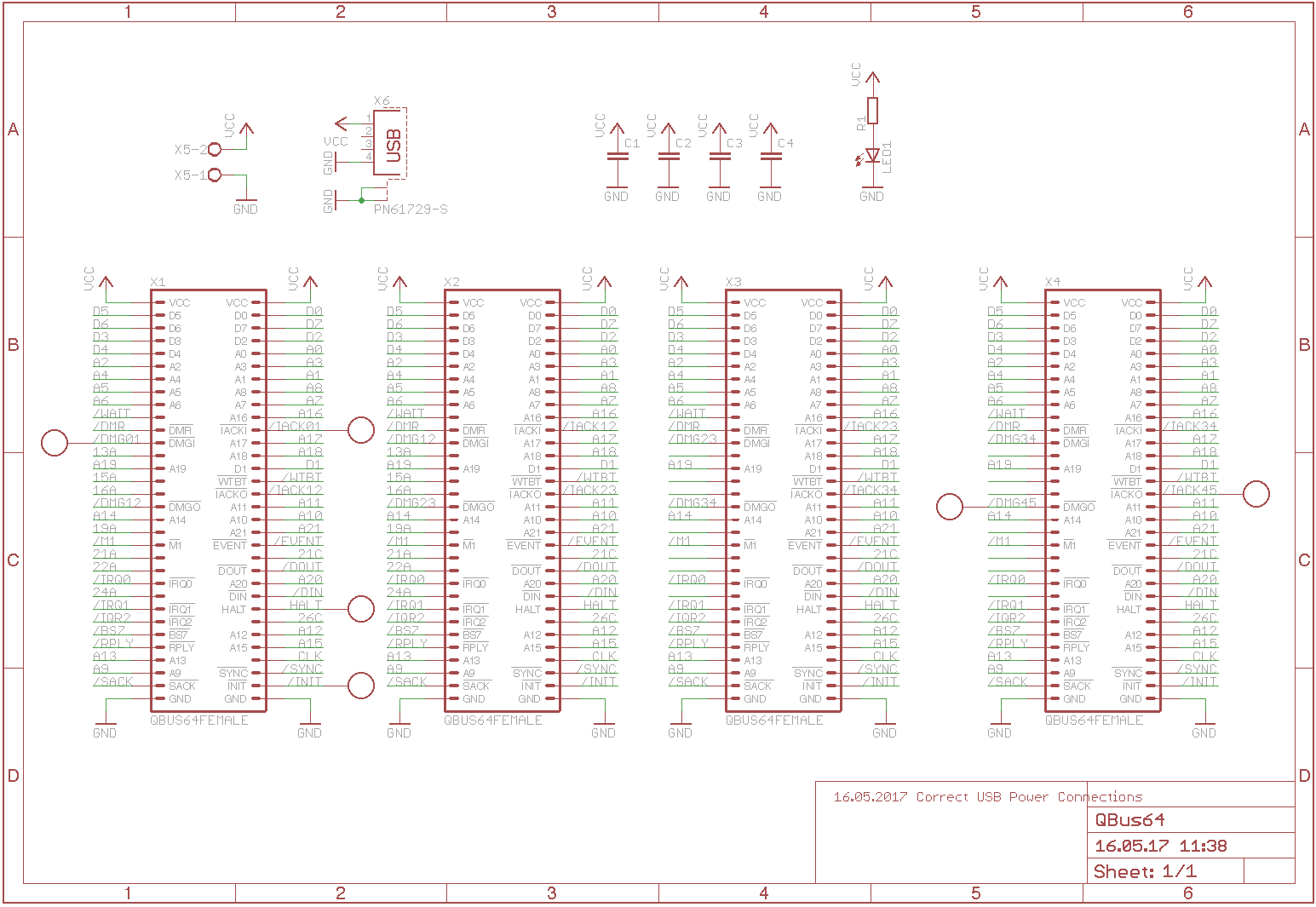
The layout of the system bus is based on the ECB bus. It uses DIN41612 connectors with two rows: a+c. The bus protocol is based on the Q-Bus. I tried to map all Q-Bus signals to ECB bus signals with similar functionality. As with the Q-Bus the address and data are multiplexed. Mostly because the DCJ11 uses the same multiplexing of address and data. Contrary to the Q-Bus the address/data bus uses positive logic and tri-state buffers. The other signals however use negative logic and open collector. Like the Q-Bus the ECB bus also has two daisy chain signals for interrupt and DMA processing.
I named the system bus the QBUS64
The reason I chose the Q-Bus was that I wanted to be able to use standard PDP-11 software. I considered that the closer the hardware matches the real PDP-11 the more likely the software will run. Also I wanted to have an asynchronous bus so I did not have to use a system clock. And I wanted to be able to add and remove IO boards without having to change any system configuration, i.e. like with a real PDP-11 the software could detect whether an address was valid or not. Even the breadboard version already implemented the bus timeout to support the detection of valid memory and device addresses.
CPU Board
The CPU board consists of the DCJ11 some latches, bus transceivers and RAM. The glue logic is implemented using a single ATF1508 CPLD. A microcontroller supervisory IC has been added to generate a decent reset signal and adds battery backup to the RAM. The RAM is using AS6C8016 static RAM which are 512k x 16bit SRAM with byte support. The CPU board can be equipped with either one or two memory chips giving it a memory size of either 1 or 2 Mbyte. The current system has only 1 Mbyte, sufficient to boot my favorite OS RSX-11M-Plus
Multifunction Board
The multifunction board has the following features- BootROM
- LTC Register
- TOY (compatible with the clock of the PDP-11/93) using a DS1215 RTC
- Console
- DLV11J
RLV12 Emulator
Emulates a RLV12 controller with four attached units. Units can be either a RL01 or RL02. The emulator uses a SD-Card to store the disk images. Disk images can either be dedicated partitions on the SD-Card or they can be disk image files in a FAT-32 partition. It also supports mixed configuration.
Later I have ported the RLV12 Emulator to the real Q-Bus. Both models are described in more detailed in its dedicated pages.
Board Design
The boards were all designed using Eagle. I’m limited to Euro-Card sized PCBs due to the license I use. All boards are 2 Layer boards.