MCU based IO card
Introduction
As mentioned before, the ultimate goal is to run RT-11 from a TU-58 tape. For this I have designed a small expansion card that uses a CPLD ATF1508 and a microcontroller AVR128DB64. The CPLD connects to all expansion slot signals and has an interface to the microcontroller. The microcontroller connects to the data bus and of to the CPLD via the before mentioned interface. The design follows many ideas from my RLV12 emulators. In this chapter I will just present the schematics. The following chapters will gradually add more and more features to the CPLD and eventually start with the firmware of the microcontroller and explain the section of the schematic used for each step.

The AVR128DB64 provides a multi-voltage IO port, which is port C. This is very useful, when you have to interface to devices operated at multiple voltages. In our case the MCU operates at 5V as it mostly interfaces with the DCJ11 and the CPLD which operates at 5v as well. Because SD-Cards operate at 3V3 and I want to interface the MCU IO board with an SD-Card in the future, port C is operated at 3V3 using a LDO voltage regulator. Port C provide the SPI to the SD-Card and USART1 that is used to interact with the MCU directly during debugging and configuration. The USART is galvanically isolated using a ADUM1201. When using a USB to TTL/Serial adapter the adapter must provide power to the ADUM1201. The voltage provided by the adapter must be in the range of 3V to 5V.
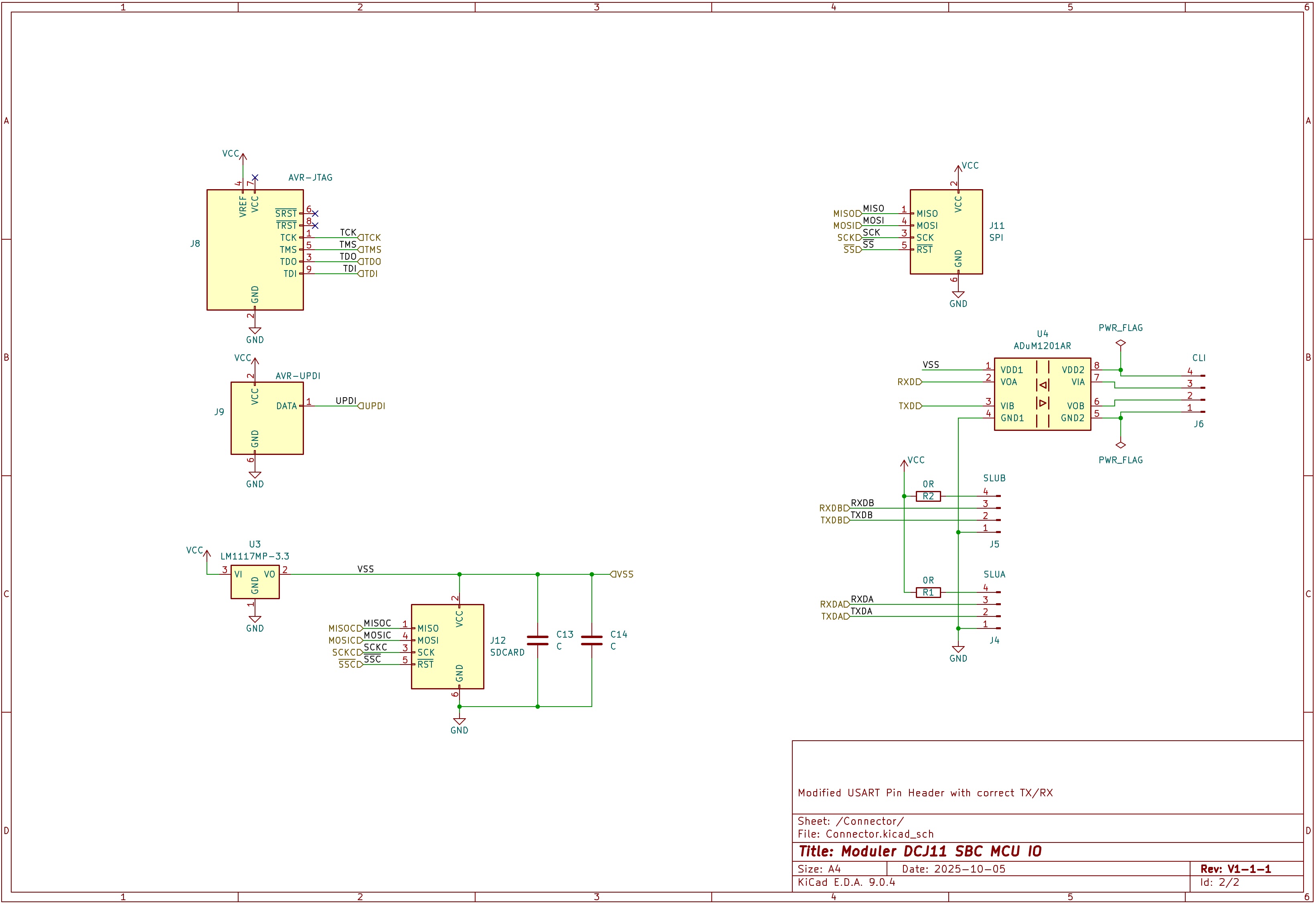
The following shows the first version of the MCU IO based expansion card with the minimal components installed. These are the MCU, the CPLD, the programming connectors for both, the pin header for the serial MCU interface, the voltage regulator to create the 3V3 used for the MVIO port.

Note, the CPLD and the microcontroller have a TQFP package with a 0.5mm pitch. Also you will need programmers for the CPLD and the microcontroller. You can also order the PCB with the TQFP packages already assembled. Many manufacturer offer the option to partially assemble PCBs. All other components are either SMD parts that are easy to solder or through hole parts.
CPLD Pin Assignement
Throughout all examples the header section of the CPLD design file is the same. It includes the device header, pin allocation, definition and fields. WinCUPL does not care whether an assignement is used or not.
Name     DCJ11MCUx;
PartNo   00 ;
Date     08.08.2025 ;
Revision 01 ;
Designer cbscpe ;
Company  PRIVAT ;
Assembly None ;
Location Switzerland ;

Device   f1508isptqfp100 ;

PROPERTY ATMEL {preassign = KEEP};
PROPERTY ATMEL {open_collector=ABORT};

/*
	Expansion Card with CPLD and MCU for MCU based IO

	A series of experiments using the MCU-V1-1 expansion card to gradually
	build a full blown PDP-11 using the DCJ11 SBC V1-3-x

 */
PIN        78 =  DAL0;		/* Data/Address Line				*/
PIN        77 =  DAL1;		/* Data/Address Line				*/
PIN        76 =  DAL2;		/* Data/Address Line				*/
PIN        68 =  DAL3;		/* Data/Address Line				*/
PIN        67 =  DAL4;		/* Data/Address Line				*/
PIN        65 =  DAL5;		/* Data/Address Line				*/
PIN        64 =  DAL6;		/* Data/Address Line				*/
PIN        63 =  DAL7;		/* Data/Address Line				*/
PIN        61 =  DAL8;		/* Data/Address Line				*/
PIN        60 =  DAL9;		/* Data/Address Line				*/
PIN        58 =  DAL10;		/* Data/Address Line				*/
PIN        57 =  DAL11;		/* Data/Address Line				*/
PIN        56 =  DAL12;		/* Data/Address Line				*/
PIN        55 =  DAL13;		/* Data/Address Line				*/
PIN        54 =  DAL14;		/* Data/Address Line				*/
PIN        53 =  DAL15;		/* Data/Address Line				*/

PIN         1 =  LAIO0;		/* Latched Address Input/Output			*/
PIN         2 =  LAIO1;		/* Latched Address Input/Output			*/
PIN        99 =  LAIO2;		/* Latched Address Input/Output			*/
PIN       100 =  LAIO3;		/* Latched Address Input/Output			*/

PIN        97 =  LBS0;		/* Latched Bank Select				*/
PIN        98 =  LBS1;		/* Latched Bank Select				*/

PIN        90 = !ALE;		/* Address Latch Enable				*/
PIN        93 = !BUFCTL;
PIN        92 = !CONT;		/* 						*/
PIN        10 = !ABORT;		/* 						*/
PIN        84 =  HALT;		/* 						*/
PIN        94 =  DV;		/* 						*/
PIN        96 = !SCTL;
PIN        89 = !STRB;
PIN         8 = !MISS;		/* 						*/
PIN        85 =  CLK;
PIN         5 =  INIT;
PIN         7 = !PWRF;
PIN         9 = !MAP;
PIN        12 = !EVENT;		/* 						*/
PIN        13 =  IRQ0;		/* 						*/
PIN        79 =  RCVIRQC;
PIN        70 =  XMTIRQC;
PIN        71 =  BRKIRQC;
PIN        72 = !DMR;

PIN        69 = !IO;		/* 	Console IO                              */
PIN        75 = !CE;		/* 	Memory Chip Enable                      */
PIN        80 = !OE;		/* 	SBC Output Enable                       */
PIN        83 = !WEL;		/* 	SBC Write Enable Lower Byte             */
PIN        81 = !WEU;		/* 	SBC Write Enable Upper Byte             */
PIN         6 =  NXM;		/* 	Non-Existant Memory Address             */

PIN        44 =  RQST;		/* 	MCU Request Signal			*/
PIN        46 =  ACKN;
PIN        45 =  INTR;
PIN        47 =  RS0;
PIN        30 =  RS1;
PIN        88 =  RD;
PIN        87 =  WR;

PIN        42 =  DX0;		/* 	Request Information 			*/
PIN        41 =  DX1;
PIN        40 =  DX2;
PIN        37 =  DX3;
PIN        36 =  DX4;
PIN        35 =  DX5;
PIN        33 =  DX6;
PIN        32 =  DX7;

PIN        49 =  ODT;
PIN        14 =  LTC;
PIN           =  PF;

PIN        27 =  BRKA;
PIN        28 =  BRKB;
PIN        29 =  TXOB;
PIN        31 =  TXOA;
PIN        50 =  TXDB;
PIN        52 =  TXDA;

PIN        17 =  PA0;
PIN        19 =  PA1;
PIN        20 =  PA2;
PIN        21 =  PA3;
PIN        22 =  PA4;
PIN        23 =  PA5;
PIN        24 =  PA6;
PIN        25 =  PA7;

PINNODE       =  DONE;
PINNODE       =  MCUIO;
PINNODE       =  INTIO;
PINNODE       =  LEVNT;
PINNODE       =  KWIE;
PINNODE       =  LPF;
PINNODE       =  PFACK;
PINNODE       =  RXIRQC;
PINNODE       =  RXACKC;
PINNODE       =  TXIRQC;
PINNODE       =  TXACKC;

PINNODE       =  MCUIRQ;
PINNODE       =  MCUACK;

PINNODE       = [A12..0];
PINNODE       = [PF7..0];

FIELD IOADDR  = [A12..1];
FIELD GPADDR  = [A7..0];
FIELD DAL     = [DAL15..0];
FIELD LBS     = [LBS1..0];
FIELD LAIO    = [LAIO3..0];
FIELD ONBIO   = [ONBIO3..0];
FIELD IACK    = [IACK3..0];

$DEFINE AIONIO      'b'1111
$DEFINE AIOGPREAD   'b'1110
$DEFINE AIOIACK     'b'1101
$DEFINE AIOINST     'b'1100
$DEFINE AIOREAD     'b'10xx
$DEFINE AIOGPWRITE  'b'0101
$DEFINE AIOWRITE    'b'000x
$DEFINE AIOBYTE     'b'001x

$DEFINE BSMEM       'b'00
$DEFINE BSSYS       'b'01
$DEFINE BSEXT       'b'10
$DEFINE BSINT       'b'11
Preparing the DCJ11 SBC
Before you can use the MCU expansion card you need to remove the on-board glue logic which consists either of the GAL16V8 (U18) or the six TTL logic devices (U4, U7, U8, U10, U13, U14). Also you should cut the solder jumper JP4 (INIT) as we will now create INIT for the DC319 via the CPLD to make the initialization consistent with PDP-11 logic that generates a bus reset (BINIT) derived from the GPWRITES issued by the DCJ11.
First Experiment - New Glue Logic
First we will replace the glue logic, provide power-up configuration, decode some GPWRITE codes and generate ABORT.
The glue logic in the GAL16V8 provided the following singals CE, IO, OE, WEL, WEH, CONT MISS and as well GPREAD. GPREAD is not available on the expansion slot therefore we generate the power-up configuration in the CPLD.
/*
	Latch the IO address
 */

[A12..0].d    = [DAL12..0].io;
[A12..0].ck   =  ALE;

/*
	Replace on-board glue-logic, e.g. GAL16V8 or the six TTL logic devices
 */
OE            =  LAIO3 &  LAIO2 & !LAIO1 & !LAIO0          &  BUFCTL
              #  LAIO3 & !LAIO2                            &  BUFCTL;

CE            = !LBS1  & !LBS0;

IO            =  LBS1  & !LBS0  & IOADDR:['o'17756x];

WEL           = !LAIO3 & !LAIO2 & !LAIO1                   & !BUFCTL &  SCTL
              # !LAIO3 & !LAIO2 &  LAIO1          & !A0    & !BUFCTL &  SCTL;

WEU           = !LAIO3 & !LAIO2 & !LAIO1                   & !BUFCTL &  SCTL
              # !LAIO3 & !LAIO2 &  LAIO1          &  A0    & !BUFCTL &  SCTL;

/*
	Modify !CONT to stretch the CPU cycles for writes to external
	IO registers so that the write impulse for the DC319 or CDP6402
	is increased to match the requiremenets even for clock rates
	above 10MHz. By delaying CONT with SCTL for writes to external
	IO registers the write pulse will be increased from 1 to 3
	clock cycles.

	For memory access we also have to assert CONT as read-modify-write
	memory cycles use a stretched read cycle.
 */
CONT          = !LBS1 & !LBS0 &  LAIO3
              # !LBS1 & !LBS0 & !LAIO3 &  SCTL
              # !LBS1 &  LBS0
              #  LBS1 & !LBS0          &  SCTL
              #  LBS1 &  LBS0;
Power-up configuration is now generated by the CPLD as well. As we are connected to the data bus we now can generate a full 16-bit power-up code.
/*
	Power-up configuration

	As GPREAD is not available at the expansion slot we need to provide
	the power-up configuration via the CPLD.

	+---+---+---+---+---+---+---+---+---+---+---+---+---+---+---+---+
	|B15|B14|B12|B12| 0 | 0 | 0 |FPA|mod|mod|mod|mod|HLT|PU |PU |POK|
	+---+---+---+---+---+---+---+---+---+---+---+---+---+---+---+---+
	\______________/              | \_______________/ | \_______/ |
	        |                     |           |       |     |     |
	        v      		      |           |       |     |     |
	Boot address   	              |           |       |     |     |
	FPA Present <-----------------+           |       |     |     |
	Module <----------------------------------+       |     |     |
	Halt option (0=ODT, 1=Trap 4)<--------------------+     |     |
	Power Up mode <-----------------------------------------+     |
	Power OK <----------------------------------------------------+

	Power Up Mode	Description
	Bit2	Bit1
	 0	 0	PC at 24, PS at 26
	 0	 1	ODT
	 1	 0	PC=173000, PS=340
	 1	 1	User Bootstrap, =340

 */
DAL.oe        =  LAIO:[AIOGPREAD] &  BUFCTL;
DAL           =  LAIO:[AIOGPREAD] & 'b'0000000000000011;
INIT for devices is now generated by the DCJ11. For this we need to decode the GPWRITE coes that assert and de-assert the bus reset signal.
/*
	Decode GPWRITE

	Here we use STRB to latch the GPWRITE code, normally you could use
	AIO and address and latch the decoded value using ALE. However the
	expansion slot does only provide LAIO which are latched with ALE so
	we cannot use ALE. STRB on the other side is asserted after ALE.
	Also STRB has the advantage that it is active during the full CPU
	cycle not like ALE which is de-asserted in the middle of the CPU
	cycle.

	INIT using .ar and .ap
 */
INIT.ck       = 'b'0;
INIT.d        = 'b'0;
INIT.ap       =  LAIO:[AIOGPWRITE] & GPADDR:['o'014] &  STRB;
INIT.ar       =  LAIO:[AIOGPWRITE] & GPADDR:['o'214] &  STRB;
One feature I have added is a LED, which will be first used to show if the DCJ11 is running ODT. The DCJ11 always issues a special GPWRITE code when entering or leaving ODT. This is a nice feature and is as well implemented on many DCJ11 based CPU boards.
/*
	ODT using .ck and .d
 */
ODT.ck        =  LAIO:[AIOGPWRITE] & GPADDR:['o'234] &  STRB
              #  LAIO:[AIOGPWRITE] & GPADDR:['o'034] &  STRB;
ODT.d         =  A7;
MISS will be asserted for all memory access to invalid memory, i.e. wenn NXM is asserted during memory read or writes. This will cause the current CPU cycle to be stretched and will give us the opportunity to assert ABORT in the stretched part of the CPU cycle
MISS = !LBS1 & !LBS0 & NXM;
ABORT signals to the DCJ11 that a non-existing memory address or device register address has been accessed and will cause the DCJ11 to abort the CPU cycle and normally will trap through vector 010. Or in ODT will show the ? when opening the location. The signal must be asserted only during the stretched part of the CPU cycle here we use SCTL to assert ABORT as recommended in the datasheet. As noted in the comment, we need to be very specific about the cycles we need to abort.
/*
	When not implementing a time-out we need to take into account, that
	we must assert ABORT for Bank 0 only in case of read and write
	cycles. E.G. no ABORT for GPWRITES, that are also signalled with
	Bank 0, this is fatal. And the same is true for Bank 1 as interrupt
	acknowledge cycles use Bank 1. So we will very specific which cycles
	will be aborted.

 */
ABORT         = !LBS1 & !LBS0 & LAIO:[AIOINST]   &  NXM &  SCTL
              # !LBS1 & !LBS0 & LAIO:[AIOREAD]   &  NXM &  SCTL
              # !LBS1 & !LBS0 & LAIO:[AIOWRITE]  &  NXM &  SCTL
              #  LBS1 & !LBS0 & LAIO:[AIOINST]   &  NXM &  SCTL & !IO & !MCUIO
              #  LBS1 & !LBS0 & LAIO:[AIOREAD]   &  NXM &  SCTL & !IO & !MCUIO
              #  LBS1 & !LBS0 & LAIO:[AIOWRITE]  &  NXM &  SCTL & !IO & !MCUIO;
When programming the CPLD with the above equations you should now be greated by the ODT prompt and the LED should be lit when hitting the reset button.
Now you can try to run a program and the LED should turn of when you hit the G key.
And turn back on when you hit the reset button.
@0/175564 777
f@0g
000000
@
First we check if ABORT is correctly generated
@0/000777
00000002/177560
00000004/052501
00000006/052525
00000010/052525
00000012/012725
00000014/052525

@1000/125252 12737
00001002/125252 100000
00001004/125252 2000
00001006/135052 774
00001010/110212 0
00001012/001252
@777776/000200
01000000/?
@17777740/000002
@17777752/000000
@17773000/?
@1000/012737
00001002/100000
00001004/002000
00001006/000774
00001010/000000
@
Second we run the small program we entered above at address 1000 which writes the same value to address 2000 in a loop. This allows us to capture the bus cycles with a logic analyzer. There we should see a couple of non-stretched CPU cycles with one stretched write cycle.
Downloads
During the development of the CPLD design file and the MCU firmware I have gone through various cycles of enhancing the CPLD capabilities and the MCU firmware.
In the following archive I have collected all five stages of the CPLD design files and the corresponding JEDEC file. I included all stages primarely for documentation reasons. You either can selectively use any of the stages or you can go straight to the last generation.
The microcontroller firmware is just the newest version. Note that this is still beta and though it fullfills the purpose of booting RT-11 from TU-58 it still needs some work, therefore you should regularly look for new versions. Until the code is reasonably mature I will publish the source code, but for the moment I make only the HEX file available
The KiCad Project is a slightly modified version of the PCB that I have ordered. It corrects the wrong connection of the pin headers for SLUA and SLUB and has some minor changes to the routing. Besides that it is functionally the same board as presented.